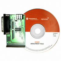
KIT33291DWEVB Freescale Semiconductor, KIT33291DWEVB Datasheet - Page 19

KIT33291DWEVB
Manufacturer Part Number
KIT33291DWEVB
Description
KIT EVAL FOR MC33291 SMART SW
Manufacturer
Freescale Semiconductor
Datasheet
1.MCZ33291EGR2.pdf
(27 pages)
Specifications of KIT33291DWEVB
Main Purpose
Power Management, Low Side Driver (Internal FET)
Embedded
No
Utilized Ic / Part
MC33291
Primary Attributes
8 Channel Internal Switch
Secondary Attributes
Overvoltage, Short-Circuit & Thermal Protection
Lead Free Status / RoHS Status
Contains lead / RoHS non-compliant
output voltage is less than the Output Threshold Voltage
(V
as switches, during normal operation, each MOSFET output
should either be completely turned ON or OFF. By design,
the threshold voltage was selected to be between the ON and
OFF voltage of the MOSFET. During normal operation, the
ON state V
threshold voltage and the OFF state V
than the threshold voltage. This design approach affords
using the same threshold comparator for Output Open Load
Detect in the OFF state and Short Circuit Detect in the ON
state. (See
Circuit Detect circuit.) With V
voltage of less than 3.0 V will be detected as an Output OFF
Open Load Fault while voltages greater than 4.0 V will not be
detected as a fault.
50 A, illustrated in
MOSFET drain and ground. This current source prevents the
output from floating up to V
internal wire bond failure. The internal comparator compares
the drain voltage with a reference voltage, V
x V
voltage, the 33291 will declare the condition to be an open
load fault.
a false output OFF Open Load Fault may be triggered. To
prevent this false fault from being reported, an internal fault
filter in the range of 25 s to 100 s is incorporated. The
duration in which a false fault may be reported is a function of
the load impedance (R
MOSFET as well as the supply voltage (V
edge of CS triggers a built-in fault delay timer which must
time out (25 s or 100 s) before the fault comparator is
enabled to detect at faulted threshold. The circuit
automatically returns to normal operation once the condition
causing the Open Load Fault is removed.
SHORTED LOAD FAULT
output being shorted directly to supply, or an output
experiencing a current greater than the current limit.
during load short conditions providing system protection.
They are as follows:
Analog Integrated Circuit Device Data
Freescale Semiconductor
THRES
1. The output current of the device is monitored in an
2. The output current of the device is sensed by
3. The output thermal limit of the device is sensed and
An Output OFF Open Load Fault is indicates when the
The 33291 has an internal pull-down current source of
During output switching, especially with capacitive loads,
A short load, or overcurrent fault can be caused by any
There are three safety circuits progressively in operation
DD
analog fashion using a SENSEFET approach and
current limited.
monitoring the MOSFET drain voltage.
when attained causes only the specific faulted output
to be latched OFF, allowing all remaining outputs to
operate normally.
). If the output voltage is less than this reference
) of 0.6 to 0.8 x V
DS
Figure 20
voltage of the MOSFET is less than the
Figure
for an understanding of the Short
L
,C
DD
L
. Since the 33291 outputs function
19, page
,L
PWR
DD
L
), R
= 5.0 V, an OFF state output
if there is an open load or
DS(ON)
18,
DS
, and C
between the
voltage is greater
PWR
THRES
). The rising
OUT
(0.6 to 0.8
of the
output, affording robust independent output operation.
monitors the output drain current. An overcurrent condition
causes the gate control circuitry to reduce the gate-to-source
voltage imposed on the output MOSFET, re-establishing the
load current in compliance with current limit (1.0 A to 3.0 A)
range. The time required for the current limit circuitry to act is
less than 20 s. Therefore, currents higher than 1.0 A to
3.0 A will never be seen for more than 20 s (a typical
duration is 10 s). If the current of an output attempts to
exceed the predetermined limit of 1.0 A to 3.0 A (2.0 A
nominal), the V
the overcurrent comparator will be tripped as shown in
Figure
shut down immediately or continue to operate in an analog
current limited mode until either the short circuit (overcurrent)
condition is removed or thermal shutdown is reached.
protection shutdown circuitry. Consider a load short (output
short to supply) occurring on an output before, during, and
after output turn ON. When the
logic state, the corresponding output is turned ON and a
delay timer is activated. The duration of the delay timer is
70 s to 250 s. If the short circuit takes place before the
output is turned ON, the delay experienced is the entire 70 s
to 250 s followed by shutdown. If the short occurs during the
delay time, the shutdown still occurs after the delay time has
elapsed. However, if the short circuit occurs after the delay
time, shutdown is immediate (within 20 s after sensing). The
purpose of the delay timer is to prevent false faults from being
reported when switching capacitive loads.
disabled when an overcurrent is detected. The specific output
will, within 5.0 s to 10 s of encountering the short circuit, go
into an analog current limited mode. This feature is especially
All three protection mechanisms are incorporated in their
The analog current limit circuit is always active and
The status of SFPD determines whether the 33291 will
Grounding the SFPD pin will enable the short fault
If the SFPD pin is at 5.0 V (or V
20.
Analog
Figure 20. Short Circuit Detect and
Analog Current Limiting Circuit
DS
+
–
Digital
High = Fault
voltage will exceed the V
V ref
33291
2.5 to 3.5 V
+
–
V
Thres
CS
FUNCTIONAL DESCRIPTION
DD
signal rises to the high
MOSFET ON
), an output will not be
THRES
voltage and
R
Output
L
V
33291
PWR
19


