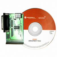
KIT33291DWEVB Freescale Semiconductor, KIT33291DWEVB Datasheet - Page 22

KIT33291DWEVB
Manufacturer Part Number
KIT33291DWEVB
Description
KIT EVAL FOR MC33291 SMART SW
Manufacturer
Freescale Semiconductor
Datasheet
1.MCZ33291EGR2.pdf
(27 pages)
Specifications of KIT33291DWEVB
Main Purpose
Power Management, Low Side Driver (Internal FET)
Embedded
No
Utilized Ic / Part
MC33291
Primary Attributes
8 Channel Internal Switch
Secondary Attributes
Overvoltage, Short-Circuit & Thermal Protection
Lead Free Status / RoHS Status
Contains lead / RoHS non-compliant
number of outputs enabled at any one time. At 25°C the
R
junction temperature to remain below 150°C, the maximum
available power dissipation must decrease as the ambient
22
33291
FUNCTIONAL DESCRIPTION
DS(ON)
The total power dissipation available is dependent on the
in 450 m with a coefficient of 6500 ppm/°C. For the
*
24-Lead
Package
SOIC
= °C/W, F = W s/°C, I PWR = W, and V A = °C
I PWR (Steady State or Transient)
(1.0 A = 1.0 W of Device Power Dissipation)
R d0
Rdx
( )*
7.0
Output 0
C d0
0.002
C
(F)*
dx
Figure 22. Thermal Model (Electrical Equivalent)
R d1
R
( )*
33
pkg
Output 1
R pkg = R leads + R PC Board
C d1
C
0.15
(F)*
pkg
R d2
Output 2
temperature increases.
of current at ambient temperatures necessary when one,
four, or eight outputs are enable ON.
how the R
temperature.
C d2
Flag Temperature Node
Junction Temperature Node
V D - T D (C°)
(Volts represent Die Surface Temperature)
Ambient Temperature Node
V A = T A (C°)
(1.0 V = 1°C Ambient Temperature)
DS(ON)
C pkg = C flag + C PC Board
output value is affected by junction
Output 6
Analog Integrated Circuit Device Data
Figure 23
R d6
C d6
depicts the per output limit
Freescale Semiconductor
Output 7
Figure 25
R d7
illustrates
C d7


