DK-SI-2SGX90N Altera, DK-SI-2SGX90N Datasheet
DK-SI-2SGX90N
Specifications of DK-SI-2SGX90N
Available stocks


Related parts for DK-SI-2SGX90N


DK-SI-2SGX90N Summary of contents
Page 1
... Transceiver SI Development Kit, 101 Innovation Drive San Jose, CA 95134 (408) 544-7000 www.altera.com P25-36005-00 Stratix II GX Edition Getting Started User Guide Development Board Version: 1.0.0 Document Version: 1.0.0 Document Date: June 2006 ...
Page 2
... Altera Corporation in the U.S. and other countries. All other product or service names are the property of their respective holders. Al- tera products are protected under numerous U ...
Page 3
... About this User Guide Revision History ......................................................................................................................................... v How to Contact Altera ............................................................................................................................... v Typographic Conventions....................................................................................................................... vi Chapter 1. About This Kit Introduction............................................................................................................................................. 1-1 Kit Features.............................................................................................................................................. 1-1 Documentation........................................................................................................................................ 1-2 Chapter 2. Getting Started Introduction............................................................................................................................................. 2-1 Before You Begin .................................................................................................................................... 2-1 Check the Kit’s Contents .................................................................................................................. 2-2 Inspect the Board............................................................................................................................... 2-2 Hardware Requirements ...
Page 4
... Write and Read PMA values................................................................................................................ A-6 Write PMA Values ........................................................................................................................... A-6 Read PMA Values ............................................................................................................................ A-6 Design Walkthrough With Troubleshooting and Debugging Solutions....................................... A-7 Design Walkthrough ........................................................................................................................ A-7 Troubleshooting................................................................................................................................ A-7 Signal TAP II File.............................................................................................................................. A-8 Creating Your Custom Data Generators and Checkers ................................................................... A-9 4 Preliminary Stratix Device Handbook, Volume 1 Altera Corporation ...
Page 5
... This user guide provides getting started information about the Altera Stratix How to Contact For the most up-to-date information about Altera products the Altera world-wide web site at www.altera.com. For technical support on Altera this product www.altera.com/mysupport. For additional information about Altera products, consult the sources shown below. ...
Page 6
... The feet direct you to more information on a particular topic. 6 Preliminary Meaning , \qdesigns directory, d: drive, chiptrip.gdf file. MAX , PIA input. , Active-low signals are denoted by suffix c:\qdesigns\tutorial\chiptrip.gdf SUBDESIGN ), as well as logic function names (e.g., data1 , n resetn , e.g Also, sections of an TRI ) are shown in Altera Corporation June 2006 ...
Page 7
... Transceiver SI Development Kit Application & Drivers—The kit’s application and drivers allow you to customize board designs by choosing transceiver settings from a wide list of categories. Quartus II Software, Development Kit Edition (DKE)—The Quartus II software provides a comprehensive environment for system-on-a- programmable-chip (SOPC) design. The Quartus II software integrates into nearly any design environment, with interfaces to industry-standard EDA tools ...
Page 8
... Transceiver Signal Integrity Development Kit, Stratix II GX Edition 1 The Quartus II DKE software license allows you to use the product for 12 months. After 12 months, you must purchase a renewal subscription to continue using the software. For more information, refer to the Altera www.altera.com. ...
Page 9
... Begin listed in this section. If any of the items are missing, contact Altera you proceed. You should also verify that your computer’s hardware and software meet the kit’s system requirements. ...
Page 10
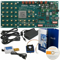
... Transceiver Signal Integrity Development Kit, Stratix II GX Edition Stratix II GX transceiver signal integrity development board with an EP2SGX90EF1152C3NES Stratix II GX device (ordering code: DK-SI-2SGX90N) Transceiver SI Development Kit, Stratix II GX Edition CD-ROM, version 1.0.0, which includes: Reference design ● Stratix II GX signal integrity development kit application and ● ...
Page 11
... Hardware Requirements All of the hardware that you need to use the board is provided with the Transceiver Signal Integrity Development Kit, Stratix II GX Edition. Altera Corporation June 2006 shows the Stratix II GX EP2SGX90 transceiver signal integrity 50-MHz Oscillator Used for System Clock (U10) ...
Page 12
... Quartus II software provided with the kit, your system must meet the Quartus II software minimum requirements. f For system requirements, refer to the Quartus II Installation & Licensing for PCs at www.altera.com. 2–4 Transceiver Signal Integrity Development Kit, Stratix II GX Edition The Quartus II software version 6.0. See Software and MegaCore Functions” ...
Page 13
... The installation program copies the Transceiver SI Development Kit, Stratix II GX Edition files to your hard-disk, installs the software driver and application, and creates an icon in Programs > Altera > Stratix II GX Signal Integrity Kit v1.0.0 (Windows Start menu), which you can use to launch the Windows development kit GUI. ...
Page 14
... Transceiver Signal Integrity Development Kit, Stratix II GX Edition <path> The default Windows installation directory is C:\Altera\kits. SIIGX_SI_ Kit-v1.0.0 Board_Design_Files Docs Examples lists the file directory names and a description of their Description of Contents If you receive an “Application Error” message when launching the demo application, please install version 1 ...
Page 15
... For information on obtaining a license file, refer to Considerations”. To use the Quartus II software included with the kit, you must first obtain a license file. A one year Quartus II DKE software license is included with the kit. 1 Licensing Before using the Quartus II software, you must request a license file from the Altera web site at www ...
Page 16
... Quartus II Installation & Licensing Manual for PCs, which is included with the kit. USB-Blaster download cable SMA cable Power supply cable The USB-Blaster download cable driver must be installed before the USB-Blaster download cable can be used. Getting Started User Guide Altera Corporation June 2006 ...
Page 17
... When using the clock speed DIP switch bank (S8), set switches 1-5, 7, and 8 in the closed position, and switch 6 in the open position. 1 Altera Corporation June 2006 If the board does not power up after the power cable is connected, make sure that the power switch (S10 the ON position. 2– ...
Page 18
... Designs ■ Pre-Defined Test Designs Altera engineers created a set of pre-defined test designs for you to evaluate Stratix II GX device transceiver performance and board features. As you can tell from the data listed in dramatically when choosing from various clocking schemes and data rates. ...
Page 19
... To execute the demo application’s GUI, double-click the StratixIIGX_GUI.exe file, which is available on the Transceiver SI Development Kit, Stratix II GX Edition CD-ROM. Altera Corporation June 2006 lists the allowed input clock frequency range for the various GUI Channel Data Rate Range Number 6.375 Gbps – ...
Page 20
... Transceiver Signal Integrity Development Kit, Stratix II GX Edition Before walking through the GUI tutorial, you should configure the Stratix II GX device with one of the pre-defined SOFs listed in Table 2–3. 2–5. Getting Started User Guide VCCHTX 1.5 V 1.2 V Altera Corporation June 2006 ...
Page 21
... The following list defines the analog setting parameters in the control panel window: ■ ■ ■ ■ ■ Communication Settings The top right-hand side of the control panel window provides the following Communication settings: ■ Altera Corporation June 2006 shows the jumper header connections and corresponding 5V C44 0.1µF 3 BIAS 2 OUT R45 ...
Page 22
... Display Adapters in the Device Manager window (see Figure 2–5). When the SOF is downloaded to the hardware, the link from the GUI to the board should be closed. Ch0 Pattern Ch1., Ch4 Pattern Ch5 Pattern Getting Started User Guide Figure 2–5. The Altera Corporation June 2006 ...
Page 23
... The middle center of the control panel window is the RX CRU rx_freqlocked Lock to: settings. This field shows whether the transceiver’s CRU is locked to the reference clock or to the data. When the Altera Corporation June 2006 After the serial loopback status in the GUI is changed, the Data Chk Status box may indicate Unsync’ ...
Page 24
... When this situation occurs, you should ensure that the transmitter of the channel showing Unsync’d is connected to the receiver channel by external cable or by internal serial loopback. Still, when Getting Started User Guide Altera Corporation June 2006 ...
Page 25
... The following lists the required test equipment: ■ ■ ■ f For information on using Altera megafunctions to customize transceiver channels, refer to the Stratix II GX alt2gxb Megafunction User Guide chapter of the Stratix II GX Device Handbook, Volume 2. Set Up The Testing Environment This section provides the steps in setting up a testing environment. ...
Page 26
... TX_P0, and TX_N0. For the trigger clock output from the Stratix II GX transceiver signal integrity board, use the DC block. Also use the attenuator depending on the allowable input voltage range of the oscilloscope. Getting Started User Guide Altera Corporation June 2006 ...
Page 27
... Figure 2–6. Connecting the TDS8000 Sampling Oscilloscope TX_P0 TX_N0 f For more information, please refer to the Tektronix TDS8000 User Guide or reference manual of the sampling oscilloscope used. Altera Corporation June 2006 TDS 8000 Sampling Scope Basic_trig_clock Getting Started User Guide Transceiver Signal Integrity Development Kit, Stratix II GX Edition Getting Started 2– ...
Page 28
... Measuring Signal Eye Diagrams of Transmitted Data 2–20 Transceiver Signal Integrity Development Kit, Stratix II GX Edition Getting Started User Guide Altera Corporation June 2006 ...
Page 29
... MHz. Please set switch 6 in the clock setting DIP switch bank (S8) to OPEN. position. Figure A–1. Clock Setting DIP Switch Bank (All Switches In Closed Position) Altera Corporation June 2006 Appendix A. Non-GUI Based The checkers are only available for the PRBS23 and PRBS7 data patterns. Preemphasis— ...
Page 30
... The LED is reset when clear_error_counter_switch is asserted. Getting Started User Guide Table A–1 lists the Board Connected Width Reference to FPGA Pin Number Number 1 D1 AE33 1 D2 AE32 1 D3 AD26 1 D4 AD25 1 D5 AD34 1 D6 AE34 1 D7 AC29 Altera Corporation June 2006 ...
Page 31
... DIP Switches The DIP switch S7 is used for controlling the different transceiver parameters. individual switch functions. The DIP switch numbers are shown on the board’s silkscreen. Altera Corporation June 2006 Description The LED is ON when serial loopback is enabled Display the VOD, pre-emphasis, DC gain, and equalization values when reading or writing the PMA settings. “ ...
Page 32
... DIP switch bank. Note (1) Description Getting Started User Guide Board Connected Width Reference to FPGA Pin Number Number 1 1 AH33 AH32, AF28, AF27 AJ34, AJ33 1 7 AG29 1 8 AG28 Altera Corporation June 2006 ...
Page 33
... Push Button Switch Name resetn (system reset) generator_checker_reset_switch change_PMA_switch insert_error_switch clear_error_counter_switch show error count Altera Corporation June 2006 lists the push button switch signal names, describes the Description Performs a reset on the transceiver and also the entire design. Performs a reset on the data generators and error checkers ...
Page 34
... Set PMA_controls (DIP_sw[3,2,1]) DIP switch to preemphasis, VOD, equalization gain settings. “DIP Switches” on page A–3 Observe the values in the 7-segment display. The value read from the transceiver is displayed. Getting Started User Guide for the values. for more information. for the values. Altera Corporation June 2006 ...
Page 35
... Refer Altera Corporation June 2006 Please refer to “Stratix II GX Transceiver Signal Integrity Development Board” on page 2–3 references. Power up the board. If the on-board clock is used, ensure that the slide switch (S9 the oscillator position (OSC). Set switch 6 of the clock setting DIP switch bank (S8) to OPEN. ...
Page 36
... Inputs and outputs of VOD, preemphasis, equalization and DC ● gain values Read, write, busy, and data valid signals ● Data generator and checker signals Parallel data output to the transceiver ● Getting Started User Guide ® II Embedded Logic Analyzer Altera Corporation June 2006 ...
Page 37
... The data output of this module should be connected to the tx_datain port Generators and of the transceiver instantiation (alt2gxb_6G_6250.v) in the top-level Checkers design_s2gx_top_level.v. Altera Corporation June 2006 Data pattern selected by the DIP switch, which have the ● following values: • ...
Page 38
... Creating Your Custom Data Generators and Checkers A–10 Transceiver Signal Integrity Development Kit, Stratix II GX Edition Getting Started User Guide Altera Corporation June 2006 ...