IRF9Z20 Vishay, IRF9Z20 Datasheet
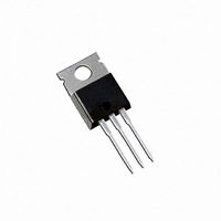
MOSFET P-CH 50V 9.7A TO-220AB

IRF9Z20

Manufacturer Part Number
IRF9Z20
Description
MOSFET P-CH 50V 9.7A TO-220AB
Manufacturer
Vishay
Datasheet

Specifications of IRF9Z20

Fet Type
MOSFET P-Channel, Metal Oxide
Fet Feature
Standard
Rds On (max) @ Id, Vgs
280 mOhm @ 5.6A, 10V
Drain To Source Voltage (vdss)
50V
Current - Continuous Drain (id) @ 25° C
9.7A
Vgs(th) (max) @ Id
4V @ 250µA
Gate Charge (qg) @ Vgs
26nC @ 10V
Input Capacitance (ciss) @ Vds
480pF @ 25V
Power - Max
40W
Mounting Type
Through Hole
Package / Case
TO-220-3 (Straight Leads)
Lead Free Status / RoHS Status
Contains lead / RoHS non-compliant
Other names
*IRF9Z20

Available stocks

Company
Part Number
Manufacturer
Quantity
Price
Part Number:
IRF9Z20
Manufacturer:
IR
Quantity:
8 000
Part Number:
IRF9Z20
Manufacturer:
IR
Quantity:
20 000
Part Number:
IRF9Z20PBF
Manufacturer:
Vishay/Siliconix
Quantity:
1 863
Notes
a. Repetitive rating; pulse width limited by maximum junction temperature (see fig. 14).
b. V
c. 0.063" (1.6 mm) from case.
* Pb containing terminations are not RoHS compliant, exemptions may apply
Document Number: 90121
S09-0074-Rev. A, 02-Feb-09
PRODUCT SUMMARY
V
R
Q
Q
Q
Configuration
ORDERING INFORMATION
Package
Lead (Pb)-free
SnPb
ABSOLUTE MAXIMUM RATINGS T
PARAMETER
Drain-Source Voltage
Gate-Source Voltage
Continuous Drain Current
Pulsed Drain Current
Linear Derating Factor
Inductive Current, Clamped
Unclamped Inductive Current (Avalanche Current)
Maximum Power Dissipation
Operating Junction and Storage Temperature Range
Soldering Recommendations (Peak Temperature)
DS
DS(on)
g
gs
gd
DD
(Max.) (nC)
(nC)
(nC)
(V)
= - 25 V, starting T
(Ω)
TO-220
G
a
D
J
S
= 25 °C, L =100 µH, R
V
GS
= - 10 V
G
P-Channel MOSFET
Single
- 50
6.2
8.6
26
G
= 25 Ω
S
D
C
Power MOSFET
V
0.28
= 25 °C, unless otherwise noted
GS
at - 10 V
L = 100 µH
T
C
for 10 s
= 25 °C
T
T
C
C
TO-220
IRF9Z20PbF
SiHF9Z20-E3
IRF9Z20
SiHF9Z20
= 100 °C
= 25 °C
FEATURES
• P-Channel Versatility
• Compact Plastic Package
• Fast Switching
• Low Drive Current
• Ease of Paralleling
• Excellent Temperature Stability
• Lead (Pb)-free Available
DESCRIPTION
The Power MOSFET technology is the key to Vishay’s
advanced line of Power MOSFET transistors. The efficient
geometry and unique processing of the Power MOSFET
design achieve very low on-state resistance combined with
high transconductance and extreme device ruggedness.
The P-Channel Power MOSFET’s are designed for
application which require the convenience of reverse polarity
operation. They retain all of the features of the more common
N-Channel Power MOSFET’s such as voltage control, very
fast switching, ease of paralleling, and excellent temperature
stability.
P-Channel Power MOSFETs are intended for use in power
stages where complementary symmetry with N-Channel
devices offers circuit simplification. They are also very useful
in drive stages because of the circuit versatility offered by the
reverse polarity connection. Applications include motor
control, audio amplifiers, switched mode converters, control
circuits and pulse amplifiers.
SYMBOL
T
J
V
V
I
I
P
, T
I
DM
LM
I
DS
GS
D
L
D
stg
IRF9Z20, SiHF9Z20
- 55 to + 150
LIMIT
± 20
- 9.7
- 6.1
0.32
- 2.2
300
- 50
- 39
- 39
40
Vishay Siliconix
c
www.vishay.com
UNIT
W/°C
RoHS*
COMPLIANT
°C
W
V
A
A
A
Available
1

Related parts for IRF9Z20

IRF9Z20 Summary of contents

Page 1

... Applications include motor control, audio amplifiers, switched mode converters, control circuits and pulse amplifiers. TO-220 IRF9Z20PbF SiHF9Z20-E3 IRF9Z20 SiHF9Z20 = 25 °C, unless otherwise noted ° 100 ° 100 µ °C C for Ω G IRF9Z20, SiHF9Z20 Vishay Siliconix SYMBOL LIMIT ± ...

Page 2

... IRF9Z20, SiHF9Z20 Vishay Siliconix THERMAL RESISTANCE RATINGS PARAMETER Maximum Junction-to-Ambient Case-to-Sink, Flat, Greased Surface Maximum Junction-to-Case (Drain) SPECIFICATIONS °C, unless otherwise noted J PARAMETER Static Drain-Source Breakdown Voltage Gate-Source Threshold Voltage Gate-Source Leakage Zero Gate Voltage Drain Current Drain-Source On-State Resistance Forward Transconductance ...

Page 3

... Pulse Test - Negative V Drain-to-Source Voltage ( Fig Typical Saturation Characteristics 3 10 Operation in this area limited DS(on IRF9Z20, SiHF9Z20 10 IRF9Z22, SiHF9Z22 IRF9Z20, SiHF9Z20 5 IRF9Z22, SiHF9Z22 ° 150 ° Single Pulse 0 Negative V , Drain-to-Source Voltage (V) DS Fig Maximum Safe Operating Area www.vishay.com - µs 100 µ ...

Page 4

... IRF9Z20, SiHF9Z20 Vishay Siliconix 5.0 80 µs Pulse Test < 4.0 T 3.0 2.0 1.0 0 Negative I Drain Current ( 90121_06 Fig Typical Transconductance vs. Drain Current ° 150 ° 0 Negative V , Source-to-Drain Voltage (V) 90121_07 SD Fig Typical Source-Drain Diode Forward Voltage www.vishay.com 4 ° C ° = 150 90121_08 8 10 90121_09 1 ...

Page 5

... Fig Maximum Drain Current vs. Case Temperature IRF9Z20, SiHF9Z20 Vishay Siliconix 2.0 80 µs Pulse Test 1.6 1 0 Negative I , Drain Current (A) D Fig Typical On-Resistance vs. Drain Current 10 8 IRF9Z20, SiHF9Z20 6 IRF9Z22, SiHF9Z22 100 125 T , Case Temperature (°C) C www.vishay.com = - 150 5 ...

Page 6

... IRF9Z20, SiHF9Z20 Vishay Siliconix Fig. 13a - Unclamped Inductive Test Circuit 0.5 1 0.2 0.1 0.05 0.1 0.02 0. 90121_05 Fig Maximum Effective Transient Thermal Impedance, Junction-to-Case vs. Pulse Duration Fig Switching Time Test Circuit www.vishay.com 6 Fig. 13b - Unclamped Inductive Load Test Waveforms Single Pulse ...

Page 7

... Technology and Package Reliability represent a composite of all qualified locations. For related documents such as package/tape drawings, part marking, and reliability data, see www.vishay.com/ppg?90121. Document Number: 90121 S09-0074-Rev. A, 02-Feb- 110 130 150 90121_19 Fig Typical High Temperature Reverse Bias (HTRB) IRF9Z20, SiHF9Z20 Vishay Siliconix UCL UCL 99 % UCL 2 20 FIT’s 1 130 50 70 ...

Page 8

... Vishay disclaims any and all liability arising out of the use or application of any product described herein or of any information provided herein to the maximum extent permitted by law. The product specifications do not expand or otherwise modify Vishay’ ...

Related keywords