PQ3DZ53 Sharp Microelectronics, PQ3DZ53 Datasheet
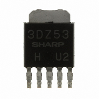
PQ3DZ53
Specifications of PQ3DZ53
Available stocks


Related parts for PQ3DZ53


PQ3DZ53 Summary of contents
Page 1
... Features Low power-loss (Dropout voltage : MAX. 0.5V) Surface mount package (equivalent to SC-63) Available 3.3V, 5V, 9V, 12V output type Output current (0.5A : PQ05DZ51 series/PQ3DZ53) (1.0A : PQ05DZ11 series/PQ3DZ13) Output voltage precision : ±3.0% Built-in ON/OFF control function Low dissipation current at OFF-state (Iqs : MAX. 5µA) ...
Page 2
... Output OFF-state consumption current 4 =5V, PQ05DZ51/11:V PQ3DZ53/PQ3DZ13 PQ3DZ53/13 10V, PQ05DZ51/11 16V, PQ09DZ51/11 Input voltage shall be the value when output voltage is 95% in comparison with the initial value. PQ3DZ53/13 case of opening control terminal , output voltage turns off Applied only to PQ05DZ51/11 series. 9 PQ3DZ53/PQ3DZ13: 0.02 Fig. 1 Test Circuit ...
Page 3
... =10V 0.5 1.0 Output current Io (A) Fig. 9 Overcurrent Protection Characteristics (Typical Value)(PQ05DZ11) 5.0 Vi-o=0.5V 4.0 Vi-o=1V Vi-o=2V 3.0 Vi-o=10V Vi-o=3V 2.0 Vi-o=5V 1.0 0 0.5 1.0 Output current Io (A) PQ05DZ51/11 Series / PQ3DZ53/13 Fig. 6 Overcurrent Protection Characteristics = = = =10V i O 1.5 2.0 Fig. 8 Overcurrent Protection Characteristics ...
Page 4
... PQ3DZ13 0 – 5 – 10 – 15 – 20 PQ3DZ53 – 25 – 30 – 35 – 40 – 45 – 50 – Junction temperature T PQ05DZ51/11 Series / PQ3DZ53/13 Vi-o=1V Vi-o=0.5V 1.5 2.0 PWB Material Size Cu thickness : 100 (˚C) a Fig.14 Output Voltage Deviation vs. Junction – 5 – 10 – 15 – 20 – 25 – 30 – ...
Page 5
... Input voltage V IN Fig.19 Output Voltage vs. Input Voltage (Typical Value) (PQ09DZ51) 15 Vc=2. =0. Co= =25˚ = Input voltage V (V) IN PQ05DZ51/11 Series / PQ3DZ53/13 Fig.16 Output Voltage Deviation vs. Junction –10 –20 –30 –40 –50 –60 –70 –80 –90 100 125 – (˚C) j Fig.18 Output Voltage vs. Input Voltage 7 ...
Page 6
... Input voltage V (V) IN Fig.25 Circuit Operating Current vs. Input Voltage (PQ3DZ53) 20 Vc=2. =0.33 F Co Input voltage V (V) IN PQ05DZ51/11 Series / PQ3DZ53/13 Fig.22 Output Voltage vs. Input Voltage Fig.24 Output Voltage vs. Input Voltage Fig.26 Circuit Operating Current vs. Input (Typical Value) (PQ05DZ11) Vc=2. =0. Co= =25˚ =10 ...
Page 7
... Input voltage V IN Fig.29 Circuit Operating Current vs. Input Voltage (PQ3DZ13) Vc=2. =0.33 F, Co= Input voltage V IN Fig.31 Circuit Operating Current vs. Input Voltage (PQ09DZ11) Vc=2. =0.33 F, Co= Input voltage V (V) IN PQ05DZ51/11 Series / PQ3DZ53/13 Fig.28 Circuit Operating Current vs. Input = = (V) Fig.30 Circuit Operating Current vs. Input =3 =6 ...
Page 8
... Io=0.3A, T =25˚ =0.5V(sine wave) PQ12DZ51 i(rms) RR=20 log i(rms) o(rms Input ripple frequency f (kHz) PQ05DZ51/11 Series / PQ3DZ53/13 Fig.34 Dropout Voltage vs. Junction Temperature (PQ05DZ11series/PQ3DZ13) 0.18 PO05DZ11:V PO09DZ11:V 0.17 PO12DZ11:V 0.16 PO3DZ13:V 0.15 0.14 0.13 0.12 0.11 0.10 –20 (˚C) j Fig ...
Page 9
... Output current Io (A) Typical Application DC input ON/OFF signal Model Line-ups for Tape-packaged Products Output current Sleeve-packaged products 0.5A output 1.0A output PQ05DZ51/11 Series / PQ3DZ53/13 Fig.40 Ripple Rejection vs. Output Current 100 PQ3DZ53 0.4 0 High : Output ON Low or Open: Output OFF ...
Page 10
NOTICE The circuit application examples in this publication are provided to explain representative applications of SHARP devices and are not intended to guarantee any circuit design or license any intellectual property rights. SHARP takes no responsibility for any problems related ...