ESD9R3.3ST5G ON Semiconductor, ESD9R3.3ST5G Datasheet - Page 3
ESD9R3.3ST5G
Manufacturer Part Number
ESD9R3.3ST5G
Description
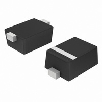
TVS ESD ULT LOW CAP SOD-923
Manufacturer
ON Semiconductor
Datasheet
1.ESD9R3.3ST5G.pdf
(4 pages)
Specifications of ESD9R3.3ST5G
Voltage - Reverse Standoff (typ)
3.3V
Voltage - Breakdown
4.8V
Power (watts)
150mW
Polarization
Unidirectional
Mounting Type
Surface Mount
Package / Case
SOD-923
Polarity
Unidirectional
Clamping Voltage
7.8 V
Operating Voltage
3.3 V
Breakdown Voltage
4.8 V
Termination Style
SMD/SMT
Peak Surge Current
1 A
Capacitance
0.5 pF
Maximum Operating Temperature
+ 125 C
Minimum Operating Temperature
- 55 C
Dimensions
0.6 mm W x 0.8 mm L
Reverse Stand-off Voltage Vrwm
3.3V
Clamping Voltage Vc Max
7.8V
Diode Configuration
Unidirectional
Peak Pulse Current Ippm
1A
Diode Case Style
SOD-923
No. Of Pins
2
Power Dissipation Pd
150mW
Rohs Compliant
Yes
Lead Free Status / RoHS Status
Lead free / RoHS Compliant
Available stocks
Company
Part Number
Manufacturer
Quantity
Price
Company:

Part Number:
ESD9R3.3ST5G
Manufacturer:
ON Semiconductor
Quantity:
55 883
Company:
Part Number:
ESD9R3.3ST5G
Manufacturer:
ON
Quantity:
30 000
Part Number:
ESD9R3.3ST5G
Manufacturer:
ON/安森美
Quantity:
20 000


The following is taken from Application Note
AND8308/D − Interpretation of Datasheet Parameters
for ESD Devices.
ESD Voltage Clamping
voltage that an IC will be exposed to during an ESD event
to as low a voltage as possible. The ESD clamping voltage
is the voltage drop across the ESD protection diode during
an ESD event per the IEC61000−4−2 waveform. Since the
IEC61000−4−2 was written as a pass/fail spec for larger
IEC 61000−4−2 Spec.
Level
For sensitive circuit elements it is important to limit the
1
2
3
4
ESD Gun
Voltage
Test
(kV)
2
4
6
8
First Peak
Current
22.5
(A)
7.5
15
30
Current at
TVS
30 ns (A)
100
90
80
70
60
50
40
30
20
10
0
12
16
4
8
0
t
Cable
Figure 4. Diagram of ESD Test Setup
50 W
r
t
Figure 5. 8 X 20 ms Pulse Waveform
P
Figure 3. IEC61000−4−2 Spec
Current at
60 ns (A)
PEAK VALUE I
20
2
4
6
8
http://onsemi.com
Oscilloscope
HALF VALUE I
50 W
t, TIME (ms)
3
RSM
PULSE WIDTH (t
AS THAT POINT WHERE THE
PEAK CURRENT DECAY = 8 ms
40
systems such as cell phones or laptop computers it is not
clearly defined in the spec how to specify a clamping voltage
at the device level. ON Semiconductor has developed a way
to examine the entire voltage waveform across the ESD
protection diode over the time domain of an ESD pulse in the
form of an oscilloscope screenshot, which can be found on
the datasheets for all ESD protection diodes. For more
information on how ON Semiconductor creates these
screenshots and how to interpret them please refer to
AND8307/D.
@ 8 ms
100%
I
peak
90%
10%
I @ 30 ns
I @ 60 ns
RSM
/2 @ 20 ms
IEC61000−4−2 Waveform
P
) IS DEFINED
60
t
P
= 0.7 ns to 1 ns
80
Related parts for ESD9R3.3ST5G
Image
Part Number
Description
Manufacturer
Datasheet
Request
R

Part Number:
Description:
ON Semiconductor [VOLTAGE REGULATOR]
Manufacturer:
ON Semiconductor
Datasheet:
Part Number:
Description:
357-036-542-201 CARDEDGE 36POS DL .156 BLK LOPRO
Manufacturer:
ON Semiconductor
Datasheet:
Part Number:
Description:
357-036-542-201 CARDEDGE 36POS DL .156 BLK LOPRO
Manufacturer:
ON Semiconductor
Datasheet:
Part Number:
Description:
357-036-542-201 CARDEDGE 36POS DL .156 BLK LOPRO
Manufacturer:
ON Semiconductor
Datasheet:
Part Number:
Description:
357-036-542-201 CARDEDGE 36POS DL .156 BLK LOPRO
Manufacturer:
ON Semiconductor
Datasheet:
Part Number:
Description:
357-036-542-201 CARDEDGE 36POS DL .156 BLK LOPRO
Manufacturer:
ON Semiconductor
Datasheet:
Part Number:
Description:
357-036-542-201 CARDEDGE 36POS DL .156 BLK LOPRO
Manufacturer:
ON Semiconductor
Datasheet:
Part Number:
Description:
357-036-542-201 CARDEDGE 36POS DL .156 BLK LOPRO
Manufacturer:
ON Semiconductor
Datasheet:
Part Number:
Description:
357-036-542-201 CARDEDGE 36POS DL .156 BLK LOPRO
Manufacturer:
ON Semiconductor
Datasheet:
Part Number:
Description:
357-036-542-201 CARDEDGE 36POS DL .156 BLK LOPRO
Manufacturer:
ON Semiconductor
Datasheet:
Part Number:
Description:
357-036-542-201 CARDEDGE 36POS DL .156 BLK LOPRO
Manufacturer:
ON Semiconductor
Datasheet:
Part Number:
Description:
Manufacturer:
ON Semiconductor
Datasheet:
Part Number:
Description:
Manufacturer:
ON Semiconductor
Datasheet:
Part Number:
Description:
Manufacturer:
ON Semiconductor
Datasheet: