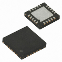
ATTINY2313V-10MU Atmel, ATTINY2313V-10MU Datasheet - Page 54

ATTINY2313V-10MU
Manufacturer Part Number
ATTINY2313V-10MU
Description
10MHZ MLF IND TEMP GREEN
Manufacturer
Atmel
Series
AVR® ATtinyr
Datasheets
1.ATTINY2313-20MU.pdf
(226 pages)
2.ATTINY2313V-10MU.pdf
(15 pages)
3.ATTINY2313V-10SU.pdf
(20 pages)
Specifications of ATTINY2313V-10MU
Core Processor
AVR
Core Size
8-Bit
Speed
10MHz
Connectivity
SPI, UART/USART
Peripherals
Brown-out Detect/Reset, POR, PWM, WDT
Number Of I /o
18
Program Memory Size
2KB (1K x 16)
Program Memory Type
FLASH
Eeprom Size
128 x 8
Ram Size
128 x 8
Voltage - Supply (vcc/vdd)
1.8 V ~ 5.5 V
Oscillator Type
Internal
Operating Temperature
-40°C ~ 85°C
Package / Case
20-MLF®, QFN
Processor Series
ATTINY2x
Core
AVR8
Data Bus Width
8 bit
Data Ram Size
128 B
Interface Type
SPI/UART/USI
Maximum Clock Frequency
10 MHz
Number Of Programmable I/os
18
Number Of Timers
2
Operating Supply Voltage
1.8 V to 5.5 V
Maximum Operating Temperature
+ 85 C
Mounting Style
SMD/SMT
Minimum Operating Temperature
- 40 C
For Use With
ATSTK600-DIP40 - STK600 SOCKET/ADAPTER 40-PDIP770-1007 - ISP 4PORT ATMEL AVR MCU SPI/JTAGATAVRDRAGON - KIT DRAGON 32KB FLASH MEM AVRATAVRISP2 - PROGRAMMER AVR IN SYSTEMATJTAGICE2 - AVR ON-CHIP D-BUG SYSTEM
Lead Free Status / RoHS Status
Lead free / RoHS Compliant
Data Converters
-
Lead Free Status / Rohs Status
Lead free / RoHS Compliant
Other names
Q2312268B
Available stocks
Company
Part Number
Manufacturer
Quantity
Price
Part Number:
ATTINY2313V-10MU
Manufacturer:
ATMEL/爱特梅尔
Quantity:
20 000
- Current page: 54 of 226
- Download datasheet (4Mb)
• DI/SDA/PCINT5 - Port B, Bit 5
DI: Three-wire mode Universal Serial Interface Data input. Three-wire mode does not override
normal port functions, so pin must be configured as an input. SDA: Two-wire mode Serial Inter-
face Data.
PCINT5: Pin Change Interrupt Source 5. The PB5 pin can serve as an external interrupt source.
• OC1B/PCINT4 – Port B, Bit 4
OC1B: Output Compare Match B output: The PB4 pin can serve as an external output for the
Timer/Counter1 Output Compare B. The pin has to be configured as an output (DDB4 set (one))
to serve this function. The OC1B pin is also the output pin for the PWM mode timer function.
PCINT4: Pin Change Interrupt Source 4. The PB4 pin can serve as an external interrupt source.
• OC1A/PCINT3 – Port B, Bit 3
OC1A: Output Compare Match A output: The PB3 pin can serve as an external output for the
Timer/Counter1 Output Compare A. The pin has to be configured as an output (DDB3 set (one))
to serve this function. The OC1A pin is also the output pin for the PWM mode timer function.
PCINT3: Pin Change Interrupt Source 3: The PB3 pin can serve as an external interrupt source.
• OC0A/PCINT2 – Port B, Bit 2
OC0A: Output Compare Match A output. The PB2 pin can serve as an external output for the
Timer/Counter0 Output Compare A. The pin has to be configured as an output (DDB2 set (one))
to serve this function. The OC0A pin is also the output pin for the PWM mode timer function.
PCINT2: Pin Change Interrupt Source 2. The PB2 pin can serve as an external interrupt source.
• AIN1/PCINT1 – Port B, Bit 1
AIN1: Analog Comparator Negative input
Configure the port pin as input with the internal pull-up
.
switched off to avoid the digital port function from interfering with the function of the analog
comparator.
PCINT1: Pin Change Interrupt Source 1. The PB1 pin can serve as an external interrupt source.
• AIN0/PCINT0 – Port B, Bit 0
AIN0: Analog Comparator Positive input. Configure the port pin as input with the internal pull-up
switched off to avoid the digital port function from interfering with the function of the Analog
Comparator.
PCINT0: Pin Change Interrupt Source 0. The PB0 pin can serve as an external interrupt source.
Table 26
and
Table 27
relate the alternate functions of Port B to the overriding signals shown in
Figure 25 on page
51. SPI MSTR INPUT and SPI SLAVE OUTPUT constitute the MISO signal,
while MOSI is divided into SPI MSTR OUTPUT and SPI SLAVE INPUT.
ATtiny2313
54
2543L–AVR–08/10
Related parts for ATTINY2313V-10MU
Image
Part Number
Description
Manufacturer
Datasheet
Request
R

Part Number:
Description:
IC MCU AVR 2K FLASH 20DIP
Manufacturer:
Atmel
Datasheet:

Part Number:
Description:
IC MCU AVR 2K FLASH 20SOIC
Manufacturer:
Atmel
Datasheet:

Part Number:
Description:
Manufacturer:
Atmel Corporation
Datasheet:

Part Number:
Description:
Manufacturer:
ATMEL Corporation
Datasheet:

Part Number:
Description:
IC MCU AVR 2K FLASH 20MLF
Manufacturer:
Atmel
Datasheet:

Part Number:
Description:
IC MCU AVR 2K FLASH 20DIP
Manufacturer:
Atmel
Datasheet:

Part Number:
Description:
IC MCU AVR 2K FLASH 20SOIC
Manufacturer:
Atmel
Datasheet:

Part Number:
Description:
IC MCU AVR 2K FLASH 20DIP
Manufacturer:
Atmel
Datasheet:

Part Number:
Description:
IC MCU AVR 2K FLASH 20SOIC
Manufacturer:
Atmel
Datasheet:

Part Number:
Description:
IC MCU AVR 2K FLASH 20SOIC
Manufacturer:
Atmel
Datasheet:

Part Number:
Description:
IC MCU AVR 2K FLASH 20WQFN
Manufacturer:
Atmel
Datasheet:

Part Number:
Description:
8-bit AVR Microcontroller with 2K Bytes In-System Programmable Flash
Manufacturer:
ATMEL Corporation
Datasheet:

Part Number:
Description:
Attiny2313 8-bit With 2k Bytes Of In-system Programmable Flash
Manufacturer:
ATMEL Corporation
Datasheet:


