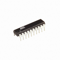
ATTINY261-20PU Atmel, ATTINY261-20PU Datasheet - Page 11

ATTINY261-20PU
Manufacturer Part Number
ATTINY261-20PU
Description
IC MCU AVR 2K FLASH 20MHZ 20-DIP
Manufacturer
Atmel
Series
AVR® ATtinyr
Specifications of ATTINY261-20PU
Core Processor
AVR
Core Size
8-Bit
Speed
20MHz
Connectivity
USI
Peripherals
Brown-out Detect/Reset, POR, PWM, WDT
Number Of I /o
16
Program Memory Size
2KB (1K x 16)
Program Memory Type
FLASH
Eeprom Size
128 x 8
Ram Size
128 x 8
Voltage - Supply (vcc/vdd)
2.7 V ~ 5.5 V
Data Converters
A/D 11x10b
Oscillator Type
Internal
Operating Temperature
-40°C ~ 85°C
Package / Case
20-DIP (0.300", 7.62mm)
Processor Series
ATTINY2x
Core
AVR8
Data Bus Width
8 bit
Data Ram Size
128 B
Interface Type
2-Wire/SPI/USI
Maximum Clock Frequency
20 MHz
Number Of Programmable I/os
16
Number Of Timers
2
Operating Supply Voltage
2.7 V to 5.5 V
Maximum Operating Temperature
+ 85 C
Mounting Style
Through Hole
3rd Party Development Tools
EWAVR, EWAVR-BL
Development Tools By Supplier
ATAVRDRAGON, ATSTK500, ATSTK600, ATAVRISP2, ATAVRONEKIT
Minimum Operating Temperature
- 40 C
On-chip Adc
11-ch x 10-bit
Data Rom Size
128 B
Height
4.95 mm
Length
26.92 mm
Supply Voltage (max)
5.5 V
Supply Voltage (min)
2.7 V
Width
7.11 mm
For Use With
ATSTK600 - DEV KIT FOR AVR/AVR32ATAVRBC100 - REF DESIGN KIT BATTERY CHARGER770-1007 - ISP 4PORT ATMEL AVR MCU SPI/JTAGATSTK505 - ADAPTER KIT FOR 14PIN AVR MCU
Lead Free Status / RoHS Status
Lead free / RoHS Compliant
Available stocks
Company
Part Number
Manufacturer
Quantity
Price
Company:
Part Number:
ATTINY261-20PU
Manufacturer:
ATMEL
Quantity:
256
- Current page: 11 of 242
- Download datasheet (5Mb)
4.5
4.5.1
4.6
2588E–AVR–08/10
Stack Pointer
Instruction Execution Timing
SPH and SPL — Stack Pointer Register
In different addressing modes these address registers function as automatic increment and
automatic decrement (see the instruction set reference for details).
The Stack is mainly used for storing temporary data, for storing local variables and for storing
return addresses after interrupts and subroutine calls. The Stack Pointer Register always points
to the top of the Stack. Note that the Stack is implemented as growing from higher memory loca-
tions to lower memory locations. This implies that a Stack PUSH command decreases the Stack
Pointer.
The Stack Pointer points to the data SRAM Stack area where the Subroutine and Interrupt
Stacks are located. This Stack space in the data SRAM must be defined by the program before
any subroutine calls are executed or interrupts are enabled. The Stack Pointer must be set to
point above 0x60. The Stack Pointer is decremented by one when data is pushed onto the Stack
with the PUSH instruction, and it is decremented by two when the return address is pushed onto
the Stack with subroutine call or interrupt. The Stack Pointer is incremented by one when data is
popped from the Stack with the POP instruction, and it is incremented by two when data is
popped from the Stack with return from subroutine RET or return from interrupt RETI.
The AVR Stack Pointer is implemented as two 8-bit registers in the I/O space. The number of
bits actually used is implementation dependent. Note that the data space in some implementa-
tions of the AVR architecture is so small that only SPL is needed. In this case, the SPH Register
will not be present
This section describes the general access timing concepts for instruction execution. The AVR
CPU is driven by the CPU clock clk
chip. No internal clock division is used.
Figure 4-4
vard architecture and the fast access Register File concept. This is the basic pipelining concept
to obtain up to 1 MIPS per MHz with the corresponding unique results for functions per cost,
functions per clocks, and functions per power-unit.
Y-register
Z-register
Bit
0x3E (0x5E)
0x3D (0x5D)
Read/Write
Initial Value
shows the parallel instruction fetches and instruction executions enabled by the Har-
15
SP15
SP7
7
R/W
R/W
RAMEND
RAMEND
15
7
R29 (0x1D)
15
7
R31 (0x1F)
14
SP14
SP6
6
R/W
R/W
RAMEND
RAMEND
13
SP13
SP5
5
R/W
R/W
RAMEND
RAMEND
CPU
ZH
YH
0
, directly generated from the selected clock source for the
12
SP12
SP4
4
R/W
R/W
RAMEND
RAMEND
RAMEND
11
SP11
SP3
3
R/W
R/W
RAMEND
0
7
R28 (0x1C)
7
R30 (0x1E)
10
SP10
SP2
2
R/W
R/W
RAMEND
RAMEND
9
SP9
SP1
1
R/W
R/W
RAMEND
RAMEND
YL
ZL
0
8
SP8
SP0
0
R/W
R/W
RAMEND
RAMEND
SPH
SPL
11
0
0
0
Related parts for ATTINY261-20PU
Image
Part Number
Description
Manufacturer
Datasheet
Request
R

Part Number:
Description:
Manufacturer:
Atmel Corporation
Datasheet:

Part Number:
Description:
Manufacturer:
Atmel Corporation
Datasheet:

Part Number:
Description:
IC MCU AVR 2K FLASH 20MHZ 32-QFN
Manufacturer:
Atmel
Datasheet:

Part Number:
Description:
MCU AVR 2K FLASH 15MHZ 32-QFN
Manufacturer:
Atmel
Datasheet:

Part Number:
Description:
MCU AVR 2KB FLASH 15MHZ 32-VQFN
Manufacturer:
Atmel
Datasheet:

Part Number:
Description:
IC MCU AVR 2K FLASH 20MHZ 20SOIC
Manufacturer:
Atmel
Datasheet:

Part Number:
Description:
Attiny261 8-bit Microcontroller With 2/4/8k Bytes In-system Programmable Flash
Manufacturer:
ATMEL Corporation
Datasheet:

Part Number:
Description:
IC MCU AVR 2K FLASH 20MHZ 20SOIC
Manufacturer:
Atmel
Datasheet:

Part Number:
Description:
IC MCU AVR 2K FLASH 20MHZ 32QFN
Manufacturer:
Atmel
Datasheet:

Part Number:
Description:
Manufacturer:
Atmel Corporation
Datasheet:


