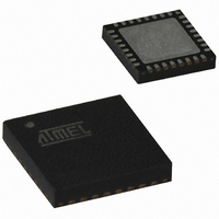
AT90PWM3-16MQ Atmel, AT90PWM3-16MQ Datasheet - Page 116

AT90PWM3-16MQ
Manufacturer Part Number
AT90PWM3-16MQ
Description
IC AVR MCU FLASH 8K 32QFN
Manufacturer
Atmel
Series
AVR® 90PWM Lightingr
Datasheet
1.AT90PWM3B-16SU.pdf
(361 pages)
Specifications of AT90PWM3-16MQ
Core Processor
AVR
Core Size
8-Bit
Speed
16MHz
Connectivity
SPI, UART/USART
Peripherals
Brown-out Detect/Reset, POR, PWM, WDT
Number Of I /o
27
Program Memory Size
8KB (8K x 8)
Program Memory Type
FLASH
Eeprom Size
512 x 8
Ram Size
512 x 8
Voltage - Supply (vcc/vdd)
2.7 V ~ 5.5 V
Data Converters
A/D 11x10b; D/A 1x10b
Oscillator Type
Internal
Operating Temperature
-40°C ~ 105°C
Package / Case
32-QFN
Processor Series
AT90PWMx
Core
AVR8
Data Bus Width
8 bit
Data Ram Size
512 B
Interface Type
SPI, USART
Maximum Clock Frequency
16 MHz
Number Of Programmable I/os
27
Number Of Timers
2
Operating Supply Voltage
2.7 V to 5.5 V
Maximum Operating Temperature
+ 105 C
Mounting Style
SMD/SMT
3rd Party Development Tools
EWAVR, EWAVR-BL
Development Tools By Supplier
ATAVRDRAGON, ATSTK500, ATSTK600, ATAVRISP2, ATAVRONEKIT, ATAVRFBKIT, ATAVRISP2
Minimum Operating Temperature
- 40 C
On-chip Adc
10 bit, 11 Channel
On-chip Dac
10 bit, 1 Channel
For Use With
ATSTK600-SOIC - STK600 SOCKET/ADAPTER FOR SOICATAVRMC200 - KIT EVAL FOR AT90PWM3 ASYNCATAVRFBKIT - KIT DEMO BALLAST FOR AT90PWM2ATAVRISP2 - PROGRAMMER AVR IN SYSTEMATSTK520 - ADAPTER KIT FOR 90PWM
Lead Free Status / RoHS Status
Lead free / RoHS Compliant
Available stocks
Company
Part Number
Manufacturer
Quantity
Price
Company:
Part Number:
AT90PWM3-16MQT
Manufacturer:
Atmel
Quantity:
1 325
- Current page: 116 of 361
- Download datasheet (7Mb)
116
AT90PWM2/3/2B/3B
Figure 15-7. Fast PWM Mode, Timing Diagram
The Timer/Counter Overflow Flag (TOVn) is set each time the counter reaches TOP. In addition
the OCnA or ICFn Flag is set at the same timer clock cycle as TOVn is set when either OCRnA
or ICRn is used for defining the TOP value. If one of the interrupts are enabled, the interrupt han-
dler routine can be used for updating the TOP and compare values.
When changing the TOP value the program must ensure that the new TOP value is higher or
equal to the value of all of the Compare Registers. If the TOP value is lower than any of the
Compare Registers, a compare match will never occur between the TCNTn and the OCRnx.
Note that when using fixed TOP values the unused bits are masked to zero when any of the
OCRnx Registers are written.
The procedure for updating ICRn differs from updating OCRnA when used for defining the TOP
value. The ICRn Register is not double buffered. This means that if ICRn is changed to a low
value when the counter is running with none or a low prescaler value, there is a risk that the new
ICRn value written is lower than the current value of TCNTn. The result will then be that the
counter will miss the compare match at the TOP value. The counter will then have to count to the
MAX value (0xFFFF) and wrap around starting at 0x0000 before the compare match can occur.
The OCRnA Register however, is double buffered. This feature allows the OCRnA I/O location
to be written anytime. When the OCRnA I/O location is written the value written will be put into
the OCRnA Buffer Register. The OCRnA Compare Register will then be updated with the value
in the Buffer Register at the next timer clock cycle the TCNTn matches TOP. The update is done
at the same timer clock cycle as the TCNTn is cleared and the TOVn Flag is set.
Using the ICRn Register for defining TOP works well when using fixed TOP values. By using
ICRn, the OCRnA Register is free to be used for generating a PWM output on OCnA. However,
if the base PWM frequency is actively changed (by changing the TOP value), using the OCRnA
as TOP is clearly a better choice due to its double buffer feature.
In fast PWM mode, the compare units allow generation of PWM waveforms on the OCnx pins.
Setting the COMnx1:0 bits to two will produce a non-inverted PWM and an inverted PWM output
can be generated by setting the COMnx1:0 to three (see
value will only be visible on the port pin if the data direction for the port pin is set as output
(DDR_OCnx). The PWM waveform is generated by setting (or clearing) the OCnx Register at
the compare match between OCRnx and TCNTn, and clearing (or setting) the OCnx Register at
the timer clock cycle the counter is cleared (changes from TOP to BOTTOM).
TCNTn
OCnx
OCnx
Period
1
2
3
4
5
6
7
Table on page
8
OCRnx/TOP Update and
TOVn Interrupt Flag Set and
OCnA Interrupt Flag Set
or ICFn Interrupt Flag Set
(Interrupt on TOP)
123). The actual OCnx
(COMnx1:0 = 2)
(COMnx1:0 = 3)
4317J–AVR–08/10
Related parts for AT90PWM3-16MQ
Image
Part Number
Description
Manufacturer
Datasheet
Request
R

Part Number:
Description:
IC AVR MCU FLASH 8K 32SOIC
Manufacturer:
Atmel
Datasheet:

Part Number:
Description:
MCU AVR 8K FLASH 16MHZ 32-QFN
Manufacturer:
Atmel
Datasheet:

Part Number:
Description:
DEV KIT FOR AVR/AVR32
Manufacturer:
Atmel
Datasheet:

Part Number:
Description:
INTERVAL AND WIPE/WASH WIPER CONTROL IC WITH DELAY
Manufacturer:
ATMEL Corporation
Datasheet:

Part Number:
Description:
Low-Voltage Voice-Switched IC for Hands-Free Operation
Manufacturer:
ATMEL Corporation
Datasheet:

Part Number:
Description:
MONOLITHIC INTEGRATED FEATUREPHONE CIRCUIT
Manufacturer:
ATMEL Corporation
Datasheet:

Part Number:
Description:
AM-FM Receiver IC U4255BM-M
Manufacturer:
ATMEL Corporation
Datasheet:

Part Number:
Description:
Monolithic Integrated Feature Phone Circuit
Manufacturer:
ATMEL Corporation
Datasheet:

Part Number:
Description:
Multistandard Video-IF and Quasi Parallel Sound Processing
Manufacturer:
ATMEL Corporation
Datasheet:

Part Number:
Description:
High-performance EE PLD
Manufacturer:
ATMEL Corporation
Datasheet:

Part Number:
Description:
8-bit Flash Microcontroller
Manufacturer:
ATMEL Corporation
Datasheet:

Part Number:
Description:
2-Wire Serial EEPROM
Manufacturer:
ATMEL Corporation
Datasheet:


