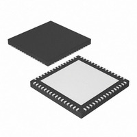
DSPIC33FJ64GS606-I/MR Microchip Technology, DSPIC33FJ64GS606-I/MR Datasheet - Page 107

DSPIC33FJ64GS606-I/MR
Manufacturer Part Number
DSPIC33FJ64GS606-I/MR
Description
IC MCU/DSP 64KB FLASH 64QFN
Manufacturer
Microchip Technology
Series
dsPIC™ 33Fr
Specifications of DSPIC33FJ64GS606-I/MR
Program Memory Type
FLASH
Program Memory Size
64KB (64K x 8)
Package / Case
64-VFQFN, Exposed Pad
Core Processor
dsPIC
Core Size
16-Bit
Speed
40 MIPs
Connectivity
CAN, I²C, IrDA, LIN, SPI, UART/USART, USB
Peripherals
Brown-out Detect/Reset, DMA, QEI, POR, PWM, WDT
Number Of I /o
58
Ram Size
9K x 8
Voltage - Supply (vcc/vdd)
3 V ~ 3.6 V
Data Converters
A/D 16x10b; D/A 1x10b
Oscillator Type
Internal
Operating Temperature
-40°C ~ 85°C
Product
DSCs
Data Bus Width
16 bit
Processor Series
DSPIC33F
Core
dsPIC
Numeric And Arithmetic Format
Fixed-Point or Floating-Point
Instruction Set Architecture
Harvard
Device Million Instructions Per Second
40 MIPs
Maximum Clock Frequency
120 MHz
Number Of Programmable I/os
58
Data Ram Size
4 KB
Operating Supply Voltage
3.3 V
Maximum Operating Temperature
+ 85 C
Mounting Style
SMD/SMT
3rd Party Development Tools
52713-733, 52714-737, 53276-922, EWDSPIC
Development Tools By Supplier
PG164130, DV164035, DV244005, DV164005, PG164120, DM240001, DV164033
Interface Type
I2C, SPI, UART
Minimum Operating Temperature
- 40 C
On-chip Adc
10 bit, 16 Channel
On-chip Dac
10 bit, 4 Channel
Lead Free Status / RoHS Status
Lead free / RoHS Compliant
Eeprom Size
-
Lead Free Status / Rohs Status
Lead free / RoHS Compliant
Available stocks
Company
Part Number
Manufacturer
Quantity
Price
Company:
Part Number:
DSPIC33FJ64GS606-I/MR
Manufacturer:
Microchip
Quantity:
176
- Current page: 107 of 418
- Download datasheet (3Mb)
4.6.2
The TBLRDL and TBLWTL instructions offer a direct
method of reading or writing the lower word of any
address within the program space without going
through data space. The TBLRDH and TBLWTH
instructions are the only method to read or write the
upper 8 bits of a program space word as data.
The PC is incremented by two for each successive
24-bit program word. This allows program memory
addresses to directly map to data space addresses.
Program memory can thus be regarded as two
16-bit-wide word address spaces, residing side by side,
each with the same address range. TBLRDL and
TBLWTL access the space that contains the least
significant data word. TBLRDH and TBLWTH access the
space that contains the upper data byte.
Two table instructions are provided to move byte or
word-sized (16-bit) data to and from program space.
Both function as either byte or word operations.
• TBLRDL (Table Read Low):
FIGURE 4-10:
2010 Microchip Technology Inc.
- In Word mode, this instruction maps the
dsPIC33FJ32GS406/606/608/610 and dsPIC33FJ64GS406/606/608/610
lower word of the program space location
(P<15:0>) to a data address (D<15:0>).
TBLPAG
02
DATA ACCESS FROM PROGRAM
MEMORY USING TABLE
INSTRUCTIONS
23
ACCESSING PROGRAM MEMORY WITH TABLE INSTRUCTIONS
15
0
0x000000
0x020000
0x030000
0x800000
Program Space
Preliminary
The address for the table operation is determined by the data EA
within the page defined by the TBLPAG register.
Only read operations are shown; write operations are also valid in
the user memory area.
TBLRDH.B (Wn<0> = 0)
TBLRDL.B (Wn<0> = 1)
TBLRDL.B (Wn<0> = 0)
TBLRDL.W
• TBLRDH (Table Read High):
Similarly, two table instructions, TBLWTH and TBLWTL,
are used to write individual bytes or words to a program
space address. The details of their operation are
explained in Section 5.0 “Flash Program Memory”.
For all table operations, the area of program memory
space to be accessed is determined by the Table Page
register (TBLPAG). TBLPAG covers the entire program
memory space of the device, including user and
configuration spaces. When TBLPAG<7> = 0, the table
page is located in the user memory space. When
TBLPAG<7> = 1, the page is located in configuration
space.
‘Phantom’ Byte
- In Byte mode, either the upper or lower byte
- In Word mode, this instruction maps the entire
- In Byte mode, this instruction maps the upper
00000000
00000000
00000000
00000000
of the lower program word is mapped to the
lower byte of a data address. The upper byte
is selected when Byte Select is ‘1’; the lower
byte is selected when it is ‘0’.
upper word of a program address (P<23:16>)
to a data address. Note that D<15:8>, the
‘phantom byte’, will always be ‘0’.
or lower byte of the program word to D<7:0>
of the data address, in the TBLRDL
instruction. The data is always ‘0’ when the
upper ‘phantom’ byte is selected (Byte
Select = 1).
23
16
8
DS70591C-page 107
0
Related parts for DSPIC33FJ64GS606-I/MR
Image
Part Number
Description
Manufacturer
Datasheet
Request
R

Part Number:
Description:
IC, DSC, 16BIT, 12KB, 40MHZ, 3.6V, DIP28
Manufacturer:
Microchip Technology
Datasheet:

Part Number:
Description:
Manufacturer:
Microchip Technology Inc.
Datasheet:

Part Number:
Description:
Manufacturer:
Microchip Technology Inc.
Datasheet:

Part Number:
Description:
Manufacturer:
Microchip Technology Inc.
Datasheet:

Part Number:
Description:
Manufacturer:
Microchip Technology Inc.
Datasheet:

Part Number:
Description:
Manufacturer:
Microchip Technology Inc.
Datasheet:

Part Number:
Description:
Manufacturer:
Microchip Technology Inc.
Datasheet:

Part Number:
Description:
Manufacturer:
Microchip Technology Inc.
Datasheet:

Part Number:
Description:
Manufacturer:
Microchip Technology Inc.
Datasheet:


