PIC16C71/JW Microchip Technology, PIC16C71/JW Datasheet - Page 63
PIC16C71/JW
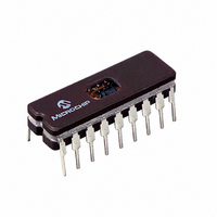
Manufacturer Part Number
PIC16C71/JW
Description
IC MCU EPROM 1KX14 A/D 18CDIP
Manufacturer
Microchip Technology
Series
PIC® 16Cr
Datasheets
1.PIC16LC711-04IP.pdf
(177 pages)
2.PIC16LC711-04IP.pdf
(8 pages)
3.PIC16C716-04P.pdf
(14 pages)
Specifications of PIC16C71/JW
Core Processor
PIC
Core Size
8-Bit
Speed
20MHz
Peripherals
POR, WDT
Number Of I /o
13
Program Memory Size
1.75KB (1K x 14)
Program Memory Type
EPROM, UV
Ram Size
36 x 8
Voltage - Supply (vcc/vdd)
4 V ~ 6 V
Data Converters
A/D 4x8b
Oscillator Type
External
Operating Temperature
0°C ~ 70°C
Package / Case
18-CDIP (0.300", 7.62mm) Window
Lead Free Status / RoHS Status
Contains lead / RoHS non-compliant
Eeprom Size
-
Connectivity
-
Other names
PIC16C71-16/JW
PIC16C71-16/JW
PIC16C71-20/JW
PIC16C71-16/JW
PIC16C71-20/JW
Available stocks
Company
Part Number
Manufacturer
Quantity
Price


8.5.1
External interrupt on RB0/INT pin is edge triggered:
either rising if bit INTEDG (OPTION<6>) is set, or fall-
ing, if the INTEDG bit is clear. When a valid edge
appears
(INTCON<1>) is set. This interrupt can be disabled by
clearing enable bit INTE (INTCON<4>). Flag bit INTF
must be cleared in software in the interrupt service rou-
tine before re-enabling this interrupt. The INT interrupt
can wake-up the processor from SLEEP, if bit INTE was
set prior to going into SLEEP. The status of global inter-
rupt enable bit GIE decides whether or not the proces-
sor branches to the interrupt vector following wake-up.
See Section 8.8 for details on SLEEP mode.
FIGURE 8-19: INT PIN INTERRUPT TIMING
1997 Microchip Technology Inc.
INSTRUCTION FLOW
Note 1: INTF flag is sampled here (every Q1).
GIE bit
(INTCON<7>)
INTF flag
(INTCON<1>)
CLKOUT
INT pin
OSC1
Instruction
executed
Instruction
fetched
PC
2: Interrupt latency = 3-4 Tcy where Tcy = instruction cycle time.
3: CLKOUT is available only in RC oscillator mode.
4: For minimum width of INT pulse, refer to AC specs.
5: INTF is enabled to be set anytime during the Q4-Q1 cycles.
INT INTERRUPT
on
Latency is the same whether Inst (PC) is a single cycle or a 2-cycle instruction.
3
the
Q1
Inst (PC-1)
RB0/INT
Inst (PC)
1
Q2
PC
Q3
4
pin,
Q4
5
Q1
flag
Inst (PC+1)
Inst (PC)
Q2
1
bit
PC+1
Q3
INTF
Q4
Interrupt Latency
Q1
Dummy Cycle
Q2
8.5.2
An overflow (FFh
flag bit T0IF (INTCON<2>). The interrupt can be
enabled/disabled by setting/clearing enable bit T0IE
(INTCON<5>). (Section 6.0)
8.5.3
An input change on PORTB<7:4> sets flag bit RBIF
(INTCON<0>). The interrupt can be enabled/disabled
by setting/clearing enable bit RBIE (INTCON<4>).
(Section 5.2)
PC+1
—
Note:
Q3
Q4
TMR0 INTERRUPT
PORTB INTCON CHANGE
2
For the PIC16C71
if a change on the I/O pin should occur
when the read operation is being executed
(start of the Q2 cycle), then the RBIF inter-
rupt flag may not get set.
Q1
Dummy Cycle
Inst (0004h)
Q2
0004h
00h) in the TMR0 register will set
Q3
PIC16C71X
Q4
Q1
DS30272A-page 63
Inst (0005h)
Q2
Inst (0004h)
0005h
Q3
Q4
Related parts for PIC16C71/JW
Image
Part Number
Description
Manufacturer
Datasheet
Request
R

Part Number:
Description:
IC, 8BIT MCU, PIC16C, 40MHZ, DIP-18
Manufacturer:
Microchip Technology
Datasheet:

Part Number:
Description:
IC, 8BIT MCU, PIC16C, 4MHZ, DIP-28
Manufacturer:
Microchip Technology
Datasheet:
Part Number:
Description:
IC, 8BIT MCU, PIC16C, 4MHZ, DIP-28
Manufacturer:
Microchip Technology
Datasheet:

Part Number:
Description:
IC, 8BIT MCU, PIC16C, 4MHZ, DIP-40
Manufacturer:
Microchip Technology
Datasheet:

Part Number:
Description:
SURFACE MOUNT POWER INDUCTORS
Manufacturer:
RCD [RCD COMPONENTS INC.]
Datasheet:

Part Number:
Description:
Manufacturer:
Microchip Technology Inc.
Datasheet:
Part Number:
Description:
Manufacturer:
Microchip Technology Inc.
Datasheet:
Part Number:
Description:
Manufacturer:
Microchip Technology Inc.
Datasheet:
Part Number:
Description:
Manufacturer:
Microchip Technology Inc.
Datasheet:
Part Number:
Description:
Manufacturer:
Microchip Technology Inc.
Datasheet:
Part Number:
Description:
Manufacturer:
Microchip Technology Inc.
Datasheet: