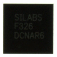
C8051F326-GM Silicon Laboratories Inc, C8051F326-GM Datasheet - Page 104

C8051F326-GM
Manufacturer Part Number
C8051F326-GM
Description
IC 8051 MCU FLASH 16K 28QFN
Manufacturer
Silicon Laboratories Inc
Series
C8051F32xr
Specifications of C8051F326-GM
Program Memory Type
FLASH
Program Memory Size
16KB (16K x 8)
Package / Case
28-QFN
Core Processor
8051
Core Size
8-Bit
Speed
25MHz
Connectivity
UART/USART, USB
Peripherals
POR
Number Of I /o
15
Ram Size
1.5K x 8
Voltage - Supply (vcc/vdd)
2.7 V ~ 3.6 V
Oscillator Type
Internal
Operating Temperature
-40°C ~ 85°C
Processor Series
C8051F3x
Core
8051
Data Bus Width
8 bit
Data Ram Size
1.5 KB
Interface Type
UART/USB
Maximum Clock Frequency
25 MHz
Number Of Programmable I/os
15
Number Of Timers
2
Operating Supply Voltage
2.7 V to 3.6 V
Maximum Operating Temperature
+ 85 C
Mounting Style
SMD/SMT
3rd Party Development Tools
PK51, CA51, A51, ULINK2
Development Tools By Supplier
C8051F320DK
Minimum Operating Temperature
- 40 C
No. Of I/o's
15
Ram Memory Size
1280Byte
Cpu Speed
25MHz
No. Of Timers
2
Digital Ic Case Style
QFN
Supply Voltage
RoHS Compliant
Package
28QFN EP
Device Core
8051
Family Name
C8051F326
Maximum Speed
25 MHz
Lead Free Status / RoHS Status
Lead free / RoHS Compliant
For Use With
770-1006 - ISP 4PORT FOR SILABS C8051F MCU336-1450 - ADAPTER PROGRAM TOOLSTICK F326336-1306 - KIT DEV FOR C8051F326/7
Eeprom Size
-
Data Converters
-
Lead Free Status / Rohs Status
Lead free / RoHS Compliant
Other names
336-1296-5
Available stocks
Company
Part Number
Manufacturer
Quantity
Price
Company:
Part Number:
C8051F326-GM
Manufacturer:
SiliconL
Quantity:
811
Part Number:
C8051F326-GMR
Manufacturer:
SILICON LABS/芯科
Quantity:
20 000
C8051F326/7
12.9. The Serial Interface Engine
The Serial Interface Engine (SIE) performs all low level USB protocol tasks, interrupting the processor
when data has successfully been transmitted or received. When receiving data, the SIE will interrupt the
processor when a complete data packet has been received; appropriate handshaking signals are automat-
ically generated by the SIE. When transmitting data, the SIE will interrupt the processor when a complete
data packet has been transmitted and the appropriate handshake signal has been received.
The SIE will not interrupt the processor when corrupted/erroneous packets are received.
12.10. Endpoint0
Endpoint0 is managed through the USB register E0CSR (Figure 12.17). The INDEX register must be
loaded with 0x00 to access the E0CSR register.
An Endpoint0 interrupt is generated when:
The E0CNT register (Figure 12.18) holds the number of received data bytes in the Endpoint0 FIFO.
Hardware will automatically detect protocol errors and send a STALL condition in response. Firmware may
force a STALL condition to abort the current transfer. When a STALL condition is generated, the STSTL bit
will be set to ‘1’ and an interrupt generated. The following conditions will cause hardware to generate a
STALL condition:
Firmware sets the SDSTL bit (E0CSR.5) to ‘1’.
12.10.1.Endpoint0 SETUP Transactions
All control transfers must begin with a SETUP packet. SETUP packets are similar to OUT packets, contain-
ing an 8-byte data field sent by the host. Any SETUP packet containing a command field of anything other
than 8 bytes will be automatically rejected by USB0. An Endpoint0 interrupt is generated when the data
from a SETUP packet is loaded into the Endpoint0 FIFO. Software should unload the command from the
Endpoint0 FIFO, decode the command, perform any necessary tasks, and set the SOPRDY bit to indicate
that it has serviced the OUT packet.
104
1. A data packet (OUT or SETUP) has been received and loaded into the Endpoint0 FIFO. The
2. An IN data packet has successfully been unloaded from the Endpoint0 FIFO and transmitted
3. An IN transaction is completed (this interrupt generated during the status stage of the transac-
4. Hardware sets the STSTL bit (E0CSR.2) after a control transaction ended due to a protocol
5. Hardware sets the SUEND bit (E0CSR.4) because a control transfer ended before firmware
1. The host sends an OUT token during a OUT data phase after the DATAEND bit has been set
2. The host sends an IN token during an IN data phase after the DATAEND bit has been set to
3. The host sends a packet that exceeds the maximum packet size for Endpoint0.
4. The host sends a non-zero length DATA1 packet during the status phase of an IN transaction.
OPRDY bit (E0CSR.0) is set to ‘1’ by hardware.
to the host; INPRDY is reset to ‘0’ by hardware.
tion).
violation.
sets the DATAEND bit (E0CSR.3).
to ‘1’.
‘1’.
Rev. 1.1


