C8051F236-GQ Silicon Laboratories Inc, C8051F236-GQ Datasheet - Page 105
C8051F236-GQ
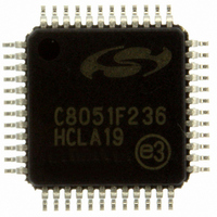
Manufacturer Part Number
C8051F236-GQ
Description
IC 8051 MCU 8K FLASH 48TQFP
Manufacturer
Silicon Laboratories Inc
Series
C8051F2xxr
Specifications of C8051F236-GQ
Program Memory Type
FLASH
Program Memory Size
8KB (8K x 8)
Package / Case
48-TQFP, 48-VQFP
Core Processor
8051
Core Size
8-Bit
Speed
25MHz
Connectivity
SPI, UART/USART
Peripherals
Brown-out Detect/Reset, POR, WDT
Number Of I /o
32
Ram Size
1.25K x 8
Voltage - Supply (vcc/vdd)
2.7 V ~ 3.6 V
Oscillator Type
Internal
Operating Temperature
-40°C ~ 85°C
Processor Series
C8051F2x
Core
8051
Data Bus Width
8 bit
Data Ram Size
1.25 KB
Interface Type
SPI/UART
Maximum Clock Frequency
25 MHz
Number Of Programmable I/os
32
Number Of Timers
3
Operating Supply Voltage
2.7 V to 3.6 V
Maximum Operating Temperature
+ 85 C
Mounting Style
SMD/SMT
3rd Party Development Tools
PK51, CA51, A51, ULINK2
Development Tools By Supplier
C8051F226DK
Minimum Operating Temperature
- 40 C
On-chip Adc
8 bit, 32 Channel
Lead Free Status / RoHS Status
Lead free / RoHS Compliant
Eeprom Size
-
Data Converters
-
Lead Free Status / Rohs Status
Lead free / RoHS Compliant
Other names
336-1244
Available stocks
Company
Part Number
Manufacturer
Quantity
Price
Company:

Part Number:
C8051F236-GQ
Manufacturer:
Silicon Laboratories Inc
Quantity:
10 000
Company:
Part Number:
C8051F236-GQR
Manufacturer:
MICROCHIP
Quantity:
2 500
Company:
Part Number:
C8051F236-GQR
Manufacturer:
Silicon Laboratories Inc
Quantity:
10 000


14.2. General Purpose Port I/O
Each I/O port is accessed through a corresponding special function register (SFR) that is both byte
addressable and bit addressable. When writing to a port, the value written to the SFR is latched to main-
tain the output data value at each pin. When reading, the logic levels of the port’s input pins are returned
regardless of the PRTnMX settings (i.e., even when the pin is assigned to another signal by the MUX, the
Port Register can always still read its corresponding Port I/O pin), provided its pin is configured for digital
input mode. The exception to this is the execution of the read-modify-write instructions. The read-modify-
write instructions when operating on a port SFR are the following: ANL, ORL, XRL, JBC, CPL, INC, DEC,
DJNZ and MOV, CLR or SETB, when the destination is an individual bit in a port SFR. For these instruc-
tions, the value of the register (not the pin) is read, modified, and written back to the SFR.
Bits7–0: P0.[7:0]
Bits7–0: PRT0CF.[7:0]: Output Configuration Bits for P0.7–P0.0 (respectively)
P0.7
R/W
Bit7
R/W
Bit7
(Write - Output appears on I/O pins per PRT0MX, PRT1MX, and PRT2MX Registers)
0: Logic Low Output.
1: Logic High Output (high impedance if corresponding PRT0CF.n bit = 0)
(Read - Regardless of PRT0MX, PRT1MX, and PRT2MX Register settings).
0: P0.n pin is logic low.
1: P0.n pin is logic high.
0: Corresponding P0.n Output mode is Open-Drain.
1: Corresponding P0.n Output mode is Push-Pull.
P0.6
SFR Definition 14.5. PRT0CF: Port0 Configuration Register
R/W
Bit6
R/W
Bit6
P0.5
R/W
Bit5
R/W
SFR Definition 14.4. P0: Port0 Register
Bit5
P0.4
R/W
Bit4
R/W
Bit4
P0.3
R/W
Bit3
Rev. 1.6
R/W
Bit3
P0.2
R/W
Bit2
R/W
Bit2
P0.1
R/W
Bit1
R/W
Bit1
(bit addressable)
C8051F2xx
P0.0
R/W
Bit0
R/W
Bit0
SFR Address:
SFR Address:
Reset Value
Reset Value
00000000
11111111
0x80
0xA4
105
Related parts for C8051F236-GQ
Image
Part Number
Description
Manufacturer
Datasheet
Request
R

Part Number:
Description:
SMD/C°/SINGLE-ENDED OUTPUT SILICON OSCILLATOR
Manufacturer:
Silicon Laboratories Inc
Part Number:
Description:
Manufacturer:
Silicon Laboratories Inc
Datasheet:
Part Number:
Description:
N/A N/A/SI4010 AES KEYFOB DEMO WITH LCD RX
Manufacturer:
Silicon Laboratories Inc
Datasheet:
Part Number:
Description:
N/A N/A/SI4010 SIMPLIFIED KEY FOB DEMO WITH LED RX
Manufacturer:
Silicon Laboratories Inc
Datasheet:
Part Number:
Description:
N/A/-40 TO 85 OC/EZLINK MODULE; F930/4432 HIGH BAND (REV E/B1)
Manufacturer:
Silicon Laboratories Inc
Part Number:
Description:
EZLink Module; F930/4432 Low Band (rev e/B1)
Manufacturer:
Silicon Laboratories Inc
Part Number:
Description:
I°/4460 10 DBM RADIO TEST CARD 434 MHZ
Manufacturer:
Silicon Laboratories Inc
Part Number:
Description:
I°/4461 14 DBM RADIO TEST CARD 868 MHZ
Manufacturer:
Silicon Laboratories Inc
Part Number:
Description:
I°/4463 20 DBM RFSWITCH RADIO TEST CARD 460 MHZ
Manufacturer:
Silicon Laboratories Inc
Part Number:
Description:
I°/4463 20 DBM RADIO TEST CARD 868 MHZ
Manufacturer:
Silicon Laboratories Inc
Part Number:
Description:
I°/4463 27 DBM RADIO TEST CARD 868 MHZ
Manufacturer:
Silicon Laboratories Inc
Part Number:
Description:
I°/4463 SKYWORKS 30 DBM RADIO TEST CARD 915 MHZ
Manufacturer:
Silicon Laboratories Inc
Part Number:
Description:
N/A N/A/-40 TO 85 OC/4463 RFMD 30 DBM RADIO TEST CARD 915 MHZ
Manufacturer:
Silicon Laboratories Inc
Part Number:
Description:
I°/4463 20 DBM RADIO TEST CARD 169 MHZ
Manufacturer:
Silicon Laboratories Inc