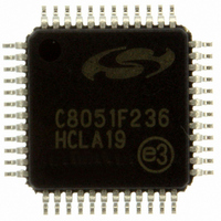
C8051F236-GQ Silicon Laboratories Inc, C8051F236-GQ Datasheet - Page 25

C8051F236-GQ
Manufacturer Part Number
C8051F236-GQ
Description
IC 8051 MCU 8K FLASH 48TQFP
Manufacturer
Silicon Laboratories Inc
Series
C8051F2xxr
Specifications of C8051F236-GQ
Program Memory Type
FLASH
Program Memory Size
8KB (8K x 8)
Package / Case
48-TQFP, 48-VQFP
Core Processor
8051
Core Size
8-Bit
Speed
25MHz
Connectivity
SPI, UART/USART
Peripherals
Brown-out Detect/Reset, POR, WDT
Number Of I /o
32
Ram Size
1.25K x 8
Voltage - Supply (vcc/vdd)
2.7 V ~ 3.6 V
Oscillator Type
Internal
Operating Temperature
-40°C ~ 85°C
Processor Series
C8051F2x
Core
8051
Data Bus Width
8 bit
Data Ram Size
1.25 KB
Interface Type
SPI/UART
Maximum Clock Frequency
25 MHz
Number Of Programmable I/os
32
Number Of Timers
3
Operating Supply Voltage
2.7 V to 3.6 V
Maximum Operating Temperature
+ 85 C
Mounting Style
SMD/SMT
3rd Party Development Tools
PK51, CA51, A51, ULINK2
Development Tools By Supplier
C8051F226DK
Minimum Operating Temperature
- 40 C
On-chip Adc
8 bit, 32 Channel
Lead Free Status / RoHS Status
Lead free / RoHS Compliant
Eeprom Size
-
Data Converters
-
Lead Free Status / Rohs Status
Lead free / RoHS Compliant
Other names
336-1244
Available stocks
Company
Part Number
Manufacturer
Quantity
Price
Company:
Part Number:
C8051F236-GQ
Manufacturer:
Silicon Laboratories Inc
Quantity:
10 000
Company:
Part Number:
C8051F236-GQR
Manufacturer:
MICROCHIP
Quantity:
2 500
Company:
Part Number:
C8051F236-GQR
Manufacturer:
Silicon Laboratories Inc
Quantity:
10 000
4.
P0.2/INT0
MONEN
P0.1/RX
P0.0/TX
XTAL1
XTAL2
Name
VREF
CP0+
CP1+
CP0-
CP1-
GND
TMS
TDO
TCK
RST
CP0
CP1
V
TDI
Pinout and Package Definitions
DD
48-Pin 32-Pin
5,6,8,
13,32
11,31
‘F206,
F220,
226,
230,
236
12
25
26
28
27
10
14
48
47
40
39
38
9
7
4
3
2
1
‘F221,
231
17
18
20
19
10
32
31
28
27
26
8
9
6
7
5
4
3
2
1
D Out JTAG Test Data Output. Data is shifted out on TDO on the falling
A Out
D Out
D Out
D I/O
A I/O
D I/O
D I/O
D I/O
Type
D In
D In
D In
D In
A In
A In
A In
A In
A In
A In
A In
A In
Table 4.1. Pin Definitions
connected (NC), but it is recommended that they be connected to
tor. Is driven low when V
voltage reference for the ADC. Otherwise, V
XTAL2. If overdriven by an external CMOS clock, this becomes
Chip Reset. Open-drain output of internal Voltage Supply moni-
Voltage Reference. When configured as an input, this pin is the
Crystal Input. This pin is the return for the internal oscillator cir-
Ground. ( Note: Pins 5,6, and 8 on the 48-pin package are not
Monitor Enable (on 48 pin package ONLY). Enables reset volt-
Port0 Bit0. (See the Port I/O Sub-System section for complete
Port0 Bit1. (See the Port I/O Sub-System section for complete
Port0 Bit2. (See the Port I/O Sub-System section for complete
JTAG Test Data Input with internal pull-up. TDI is latched on a
‘1’is written to PORSF. An external source can force a system
cuit for a crystal or ceramic resonator. For a precision internal
Crystal Output. This pin is the excitation driver for a crystal or
clock, connect a crystal or ceramic resonator from XTAL1 to
ence. NOTE: this pin is Not Connected (NC) on ‘F230/1/6.
age monitor function when pulled high (logic “1”).
Rev. 1.6
edge of TCK. TDO output is a tri-state driver.
JTAG Test-Mode Select with internal pull-up.
JTAG Test Clock with internal pull-up.
Comparator 0 Non-Inverting Input.
Comparator 1 Non-Inverting Input.
Comparator 0 Inverting Input.
Comparator 1 Inverting Input.
reset by driving this pin low.
Digital Voltage Supply.
Comparator 0 Output
Comparator 1 Output
rising edge of TCK.
ceramic resonator.
the system clock.
DD
Description
description).
description).
description).
ground.)
is < 2.7V and MONEN=1, or when a
C8051F2xx
DD
will be the refer-
25


