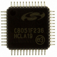
C8051F236-GQ Silicon Laboratories Inc, C8051F236-GQ Datasheet - Page 112

C8051F236-GQ
Manufacturer Part Number
C8051F236-GQ
Description
IC 8051 MCU 8K FLASH 48TQFP
Manufacturer
Silicon Laboratories Inc
Series
C8051F2xxr
Specifications of C8051F236-GQ
Program Memory Type
FLASH
Program Memory Size
8KB (8K x 8)
Package / Case
48-TQFP, 48-VQFP
Core Processor
8051
Core Size
8-Bit
Speed
25MHz
Connectivity
SPI, UART/USART
Peripherals
Brown-out Detect/Reset, POR, WDT
Number Of I /o
32
Ram Size
1.25K x 8
Voltage - Supply (vcc/vdd)
2.7 V ~ 3.6 V
Oscillator Type
Internal
Operating Temperature
-40°C ~ 85°C
Processor Series
C8051F2x
Core
8051
Data Bus Width
8 bit
Data Ram Size
1.25 KB
Interface Type
SPI/UART
Maximum Clock Frequency
25 MHz
Number Of Programmable I/os
32
Number Of Timers
3
Operating Supply Voltage
2.7 V to 3.6 V
Maximum Operating Temperature
+ 85 C
Mounting Style
SMD/SMT
3rd Party Development Tools
PK51, CA51, A51, ULINK2
Development Tools By Supplier
C8051F226DK
Minimum Operating Temperature
- 40 C
On-chip Adc
8 bit, 32 Channel
Lead Free Status / RoHS Status
Lead free / RoHS Compliant
Eeprom Size
-
Data Converters
-
Lead Free Status / Rohs Status
Lead free / RoHS Compliant
Other names
336-1244
Available stocks
Company
Part Number
Manufacturer
Quantity
Price
Company:
Part Number:
C8051F236-GQ
Manufacturer:
Silicon Laboratories Inc
Quantity:
10 000
Company:
Part Number:
C8051F236-GQR
Manufacturer:
MICROCHIP
Quantity:
2 500
Company:
Part Number:
C8051F236-GQR
Manufacturer:
Silicon Laboratories Inc
Quantity:
10 000
C8051F2xx
15.2. Operation
Only a SPI master device can initiate a data transfer. The SPI is placed in master mode by setting the
Master Enable flag (MSTEN, SPI0CN.1). Writing a byte of data to the SPI data register (SPI0DAT) when in
Master Mode starts a data transfer. The SPI master immediately shifts out the data serially on the MOSI
line while providing the serial clock on SCK. The SPIF (SPI0CN.7) flag is set to logic 1 at the end of the
transfer. If interrupts are enabled, an interrupt request is generated when the SPIF flag is set. The SPI
master can be configured to shift in/out from one to eight bits in a transfer operation in order to accommo-
date slave devices with different word lengths. The SPIFRS bits in the SPI Configuration Register
(SPI0CFG.[2:0]) are used to select the number of bits to shift in/out in a transfer operation.
While the SPI master transfers data to a slave on the MOSI line, the addressed SPI slave device simulta-
neously transfers the contents of its shift register to the SPI master on the MISO line in a full-duplex opera-
tion. The data byte received from the slave replaces the data in the master's data register. Therefore, the
SPIF flag serves as both a transmit-complete and receive-data-ready flag. The data transfer in both direc-
tions is synchronized with the serial clock generated by the master. Figure 15.3 illustrates the full-duplex
operation of an SPI master and an addressed slave.
The SPI data register is double buffered on reads, but not on a write. If a write to SPI0DAT is attempted
during a data transfer, the WCOL flag (SPI0CN.6) will be set to logic 1 and the write is ignored. The cur-
rent data transfer will continue uninterrupted. A read of the SPI data register by the system controller actu-
ally reads the receive buffer. If the receive buffer still holds unread data from a previous transfer when the
last bit of the current transfer is shifted into the SPI shift register, a receive overrun occurs and the
RXOVRN flag (SPI0CN.4) is set to logic 1. The new data is not transferred to the receive buffer, allowing
the previously received data byte to be read. The data byte causing the overrun is lost.
When the SPI is enabled and not configured as a master, it will operate as an SPI slave. Another SPI
device acting as a master will initiate a transfer by driving the NSS signal low. The master then shifts data
out of the shift register on the MOSI pin using the its serial clock. The SPIF flag is set to logic 1 at the end
of a data transfer (when the NSS signal goes high). The slave can load its shift register for the next data
transfer by writing to the SPI data register. The slave must make the write to the data register at least one
SPI serial clock cycle before the master starts the next transmission. Otherwise, the byte of data already in
the slave's shift register will be transferred.
112
7
MASTER DEVICE
SPI SHIFT REGISTER
Receive Buffer
6
Baud Rate
Generator
5
4
3
Figure 15.3. Full Duplex Operation
2
1
0
P3.0
NSS
MOSI
MISO
Rev. 1.6
SCK
SLAVE DEVICE
7
SPI SHIFT REGISTER
Receive Buffer
6
5
4
3
2
1
0


