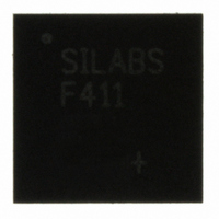
C8051F411-GM Silicon Laboratories Inc, C8051F411-GM Datasheet - Page 128

C8051F411-GM
Manufacturer Part Number
C8051F411-GM
Description
IC 8051 MCU 32K FLASH 28QFN
Manufacturer
Silicon Laboratories Inc
Series
C8051F41xr
Specifications of C8051F411-GM
Program Memory Type
FLASH
Program Memory Size
32KB (32K x 8)
Package / Case
28-QFN
Core Processor
8051
Core Size
8-Bit
Speed
50MHz
Connectivity
SMBus (2-Wire/I²C), SPI, UART/USART
Peripherals
Brown-out Detect/Reset, POR, PWM, Temp Sensor, WDT
Number Of I /o
20
Ram Size
2.25K x 8
Voltage - Supply (vcc/vdd)
2 V ~ 5.25 V
Data Converters
A/D 20x12b; D/A 2x12b
Oscillator Type
Internal
Operating Temperature
-40°C ~ 85°C
Processor Series
C8051F4x
Core
8051
Data Bus Width
8 bit
Data Ram Size
2368 B
Interface Type
I2C, SMBus, SPI, UART
Maximum Clock Frequency
50 MHz
Number Of Programmable I/os
20
Number Of Timers
4
Operating Supply Voltage
2 V to 5.25 V
Maximum Operating Temperature
+ 85 C
Mounting Style
SMD/SMT
3rd Party Development Tools
PK51, CA51, A51, ULINK2
Development Tools By Supplier
C8051F410DK
Minimum Operating Temperature
- 40 C
On-chip Adc
12 bit, 20 Channel
On-chip Dac
12 bit, 2 Channel
No. Of I/o's
20
Ram Memory Size
2368Byte
Cpu Speed
50MHz
No. Of Timers
4
Rohs Compliant
Yes
Lead Free Status / RoHS Status
Lead free / RoHS Compliant
For Use With
770-1006 - ISP 4PORT FOR SILABS C8051F MCU336-1454 - ADAPTER PROGRAM TOOLSTICK F411336-1317 - KIT EVAL FOR C8051F411336-1314 - KIT DEV FOR C8051F41X
Eeprom Size
-
Lead Free Status / Rohs Status
Lead free / RoHS Compliant
Other names
336-1309
Available stocks
Company
Part Number
Manufacturer
Quantity
Price
Company:
Part Number:
C8051F411-GM
Manufacturer:
Silicon
Quantity:
3
Part Number:
C8051F411-GM
Manufacturer:
SILICON LABS/芯科
Quantity:
20 000
Company:
Part Number:
C8051F411-GMR
Manufacturer:
SiliconL
Quantity:
3 000
Part Number:
C8051F411-GMR
Manufacturer:
SILICON LABS/芯科
Quantity:
20 000
C8051F410/1/2/3
15.1. Power-On Reset
During power-up, the device is held in a reset state and the RST pin is driven low until V
settles above
DD
V
. An additional delay occurs before the device is released from reset; the delay decreases as the V
RST
DD
ramp time increases (V
ramp time is defined as how fast V
ramps from 0 V to V
). Figure 15.2 plots
DD
DD
RST
the power-on and V
monitor reset timing. For valid ramp times (less than 1 ms), the power-on reset
DD
delay (T
) is typically less than 0.3 ms.
PORDelay
Note: The maximum V
ramp time is 1 ms; slower ramp times may cause the device to be released from
DD
reset before V
reaches the V
level.
DD
RST
On exit from a power-on reset, the PORSF flag (RSTSRC.1) is set by hardware to logic 1. When PORSF is
set, all of the other reset flags in the RSTSRC Register are indeterminate (PORSF is cleared by all other
resets). Since all resets cause program execution to begin at the same location (0x0000), software can
read the PORSF flag to determine if a power-up was the cause of reset. The contents of internal data
memory should be assumed to be undefined after a power-on reset. The V
monitor is enabled following
DD
a power-on reset.
VDD
V
RS T
1.0
t
/ RST
Logic H IG H
T
P O R D elay
Logic LO W
V D D
P ow er-O n
M onitor
R eset
R eset
Figure 15.2. Power-On and V
Monitor Reset Timing
DD
128
Rev. 1.1


