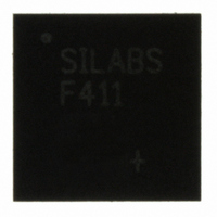
C8051F411-GM Silicon Laboratories Inc, C8051F411-GM Datasheet - Page 78

C8051F411-GM
Manufacturer Part Number
C8051F411-GM
Description
IC 8051 MCU 32K FLASH 28QFN
Manufacturer
Silicon Laboratories Inc
Series
C8051F41xr
Specifications of C8051F411-GM
Program Memory Type
FLASH
Program Memory Size
32KB (32K x 8)
Package / Case
28-QFN
Core Processor
8051
Core Size
8-Bit
Speed
50MHz
Connectivity
SMBus (2-Wire/I²C), SPI, UART/USART
Peripherals
Brown-out Detect/Reset, POR, PWM, Temp Sensor, WDT
Number Of I /o
20
Ram Size
2.25K x 8
Voltage - Supply (vcc/vdd)
2 V ~ 5.25 V
Data Converters
A/D 20x12b; D/A 2x12b
Oscillator Type
Internal
Operating Temperature
-40°C ~ 85°C
Processor Series
C8051F4x
Core
8051
Data Bus Width
8 bit
Data Ram Size
2368 B
Interface Type
I2C, SMBus, SPI, UART
Maximum Clock Frequency
50 MHz
Number Of Programmable I/os
20
Number Of Timers
4
Operating Supply Voltage
2 V to 5.25 V
Maximum Operating Temperature
+ 85 C
Mounting Style
SMD/SMT
3rd Party Development Tools
PK51, CA51, A51, ULINK2
Development Tools By Supplier
C8051F410DK
Minimum Operating Temperature
- 40 C
On-chip Adc
12 bit, 20 Channel
On-chip Dac
12 bit, 2 Channel
No. Of I/o's
20
Ram Memory Size
2368Byte
Cpu Speed
50MHz
No. Of Timers
4
Rohs Compliant
Yes
Lead Free Status / RoHS Status
Lead free / RoHS Compliant
For Use With
770-1006 - ISP 4PORT FOR SILABS C8051F MCU336-1454 - ADAPTER PROGRAM TOOLSTICK F411336-1317 - KIT EVAL FOR C8051F411336-1314 - KIT DEV FOR C8051F41X
Eeprom Size
-
Lead Free Status / Rohs Status
Lead free / RoHS Compliant
Other names
336-1309
Available stocks
Company
Part Number
Manufacturer
Quantity
Price
Company:
Part Number:
C8051F411-GM
Manufacturer:
Silicon
Quantity:
3
Part Number:
C8051F411-GM
Manufacturer:
SILICON LABS/芯科
Quantity:
20 000
Company:
Part Number:
C8051F411-GMR
Manufacturer:
SiliconL
Quantity:
3 000
Part Number:
C8051F411-GMR
Manufacturer:
SILICON LABS/芯科
Quantity:
20 000
C8051F410/1/2/3
Important Note About the V
the internal V
should be configured as an analog pin, and skipped by the Digital Crossbar. To configure P1.2 as an ana-
log pin, clear Bit 2 in register P1MDIN to ‘0’ and set Bit 2 in register P1 to '1'. To configure the Crossbar to
skip P1.2, set Bit 2 in register P1SKIP to ‘1’. Refer to
complete Port I/O configuration details. The TEMPE bit in register REF0CN enables/disables the tempera-
ture sensor. While disabled, the temperature sensor defaults to a high impedance state and any ADC0
measurements performed on the sensor result in meaningless data.
78
Bit7:
Bit6:
Bit5:
Bit4:
Bit3:
Bit2:
Bit1:
Bit0:
IDAMRG
R/W
Bit7
IDAMRG: IDAC Output Merge Select.
0: IDA1 Output is P0.1.
1: IDA1 Output is P0.0 (Merged with IDA0 Output).
GF. General Purpose Flag.
This bit is a general purpose flag for use under software control.
ZTCEN: Zero-TempCo Bias Enable Bit.
0: ZeroTC Bias Generator automatically enabled when needed.
1: ZeroTC Bias Generator forced on.
REFLV: Voltage Reference Output Level Select.
This bit selects the output voltage level for the internal voltage reference.
0: Internal voltage reference set to 1.5 V.
1: Internal voltage reference set to 2.2 V.
REFSL: Voltage Reference Select.
This bit selects the source for the internal voltage reference.
0: V
1: V
TEMPE: Temperature Sensor Enable Bit.
0: Internal Temperature Sensor off.
1: Internal Temperature Sensor on.
BIASE: Internal Analog Bias Generator Enable Bit.
0: Internal Analog Bias Generator automatically enabled when needed.
1: Internal Analog Bias Generator on.
REFBE: Internal Reference Buffer Enable Bit.
0: Internal Reference Buffer disabled.
1: Internal Reference Buffer enabled. Internal voltage reference driven on the V
REF
REF
DD
. When using either an external voltage reference or the internal reference circuitry, P1.2
R/W
GF
Bit6
used as voltage reference.
pin used as voltage reference.
SFR Definition 7.1. REF0CN: Reference Control
ZTCEN
R/W
Bit5
REF
Pin: Port pin P1.2 is used as the external V
REFLV
R/W
Bit4
Rev. 1.1
REFSL
R/W
Bit3
Section “18. Port Input/Output” on page 147
TEMPE
R/W
Bit2
BIASE
R/W
Bit1
REF
input and as an output for
REFBE
R/W
Bit0
REF
SFR Address:
00000000
Reset Value
pin.
0xD1
for


