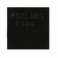
C8051F349-GM Silicon Laboratories Inc, C8051F349-GM Datasheet - Page 120

C8051F349-GM
Manufacturer Part Number
C8051F349-GM
Description
IC 8051 MCU 32K FLASH MEM 32-QFN
Manufacturer
Silicon Laboratories Inc
Series
C8051F34xr
Datasheet
1.C8051F349-GQ.pdf
(276 pages)
Specifications of C8051F349-GM
Program Memory Type
FLASH
Program Memory Size
32KB (32K x 8)
Package / Case
32-QFN
Core Processor
8051
Core Size
8-Bit
Speed
25MHz
Connectivity
SMBus (2-Wire/I²C), SPI, UART/USART, USB
Peripherals
Brown-out Detect/Reset, POR, PWM, WDT
Number Of I /o
25
Ram Size
2.25K x 8
Voltage - Supply (vcc/vdd)
2.7 V ~ 3.6 V
Oscillator Type
Internal
Operating Temperature
-40°C ~ 85°C
Processor Series
C8051F3x
Core
8051
Data Bus Width
8 bit
Data Ram Size
2304 B
Interface Type
I2C, SPI, UART
Maximum Clock Frequency
25 MHz
Number Of Programmable I/os
25
Number Of Timers
4
Operating Supply Voltage
2.7 V to 5.25 V
Maximum Operating Temperature
+ 85 C
Mounting Style
SMD/SMT
3rd Party Development Tools
KSK-SL-F34X, KSK-SL-TOOLSTICK, PK51, CA51, A51, ULINK2
Development Tools By Supplier
C8051F340DK
Minimum Operating Temperature
- 40 C
On-chip Adc
10 bit
Lead Free Status / RoHS Status
Lead free / RoHS Compliant
For Use With
336-1748 - ADAPTER TOOLSTICK FOR C8051F34X
Eeprom Size
-
Data Converters
-
Lead Free Status / Rohs Status
Lead free / RoHS Compliant
Other names
336-1349-5
Available stocks
Company
Part Number
Manufacturer
Quantity
Price
Company:
Part Number:
C8051F349-GM
Manufacturer:
Silicon Labs
Quantity:
135
- Current page: 120 of 276
- Download datasheet (2Mb)
C8051F340/1/2/3/4/5/6/7/8/9/A/B/C/D
13.5.2. Non-multiplexed Configuration
In Non-multiplexed mode, the Data Bus and the Address Bus pins are not shared. An example of a
Non-multiplexed Configuration is shown in Figure 13.3. See
page 124
13.6. Memory Mode Selection
The external data memory space can be configured in one of four modes, shown in Figure 13.4, based on
the EMIF Mode bits in the EMI0CF register (SFR Definition 13.2). These modes are summarized below.
More information about the different modes can be found in
120
EMI0CF[3:2] = 00
On-Chip XRAM
On-Chip XRAM
On-Chip XRAM
On-Chip XRAM
On-Chip XRAM
On-Chip XRAM
E
M
I
F
for more information about Non-multiplexed operation.
A[15:0]
D[7:0]
WR
RD
Figure 13.3. Non-multiplexed Configuration Example
0xFFFF
0x0000
EMI0CF[3:2] = 01
(No Bank Select)
On-Chip XRAM
Figure 13.4. EMIF Operating Modes
Off-Chip
Memory
ADDRESS BUS
DATA BUS
0xFFFF
0x0000
Rev. 1.3
(Optional)
EMI0CF[3:2] = 10
On-Chip XRAM
(Bank Select)
Off-Chip
Memory
Section “13.7.1. Non-multiplexed Mode” on
Section “13.7. Timing” on page
V
DD
8
0xFFFF
0x0000
EMI0CF[3:2] = 11
A[15:0]
I/O[7:0]
CE
WE
OE
Off-Chip
Memory
64K X 8
SRAM
122.
0xFFFF
0x0000
Related parts for C8051F349-GM
Image
Part Number
Description
Manufacturer
Datasheet
Request
R
Part Number:
Description:
SMD/C°/SINGLE-ENDED OUTPUT SILICON OSCILLATOR
Manufacturer:
Silicon Laboratories Inc
Part Number:
Description:
Manufacturer:
Silicon Laboratories Inc
Datasheet:
Part Number:
Description:
N/A N/A/SI4010 AES KEYFOB DEMO WITH LCD RX
Manufacturer:
Silicon Laboratories Inc
Datasheet:
Part Number:
Description:
N/A N/A/SI4010 SIMPLIFIED KEY FOB DEMO WITH LED RX
Manufacturer:
Silicon Laboratories Inc
Datasheet:
Part Number:
Description:
N/A/-40 TO 85 OC/EZLINK MODULE; F930/4432 HIGH BAND (REV E/B1)
Manufacturer:
Silicon Laboratories Inc
Part Number:
Description:
EZLink Module; F930/4432 Low Band (rev e/B1)
Manufacturer:
Silicon Laboratories Inc
Part Number:
Description:
I°/4460 10 DBM RADIO TEST CARD 434 MHZ
Manufacturer:
Silicon Laboratories Inc
Part Number:
Description:
I°/4461 14 DBM RADIO TEST CARD 868 MHZ
Manufacturer:
Silicon Laboratories Inc
Part Number:
Description:
I°/4463 20 DBM RFSWITCH RADIO TEST CARD 460 MHZ
Manufacturer:
Silicon Laboratories Inc
Part Number:
Description:
I°/4463 20 DBM RADIO TEST CARD 868 MHZ
Manufacturer:
Silicon Laboratories Inc
Part Number:
Description:
I°/4463 27 DBM RADIO TEST CARD 868 MHZ
Manufacturer:
Silicon Laboratories Inc
Part Number:
Description:
I°/4463 SKYWORKS 30 DBM RADIO TEST CARD 915 MHZ
Manufacturer:
Silicon Laboratories Inc
Part Number:
Description:
N/A N/A/-40 TO 85 OC/4463 RFMD 30 DBM RADIO TEST CARD 915 MHZ
Manufacturer:
Silicon Laboratories Inc
Part Number:
Description:
I°/4463 20 DBM RADIO TEST CARD 169 MHZ
Manufacturer:
Silicon Laboratories Inc


