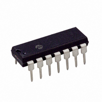
PIC16F684-E/P Microchip Technology, PIC16F684-E/P Datasheet - Page 61

PIC16F684-E/P
Manufacturer Part Number
PIC16F684-E/P
Description
IC PIC MCU FLASH 2KX14 14DIP
Manufacturer
Microchip Technology
Series
PIC® 16Fr
Datasheets
1.PIC16F616T-ISL.pdf
(8 pages)
2.PIC16F688T-ISL.pdf
(688 pages)
3.PIC16F684-ISL.pdf
(4 pages)
4.PIC16F684-ISL.pdf
(192 pages)
5.PIC16F684-ISL.pdf
(6 pages)
6.PIC16F684-IST.pdf
(164 pages)
Specifications of PIC16F684-E/P
Program Memory Type
FLASH
Program Memory Size
3.5KB (2K x 14)
Package / Case
14-DIP (0.300", 7.62mm)
Core Processor
PIC
Core Size
8-Bit
Speed
20MHz
Peripherals
Brown-out Detect/Reset, POR, PWM, WDT
Number Of I /o
12
Eeprom Size
256 x 8
Ram Size
128 x 8
Voltage - Supply (vcc/vdd)
2 V ~ 5.5 V
Data Converters
A/D 8x10b
Oscillator Type
Internal
Operating Temperature
-40°C ~ 125°C
Processor Series
PIC16F
Core
PIC
Data Bus Width
8 bit
Data Ram Size
128 B
Maximum Clock Frequency
20 MHz
Number Of Programmable I/os
12
Number Of Timers
3
Operating Supply Voltage
2 V to 5.5 V
Maximum Operating Temperature
+ 125 C
Mounting Style
Through Hole
3rd Party Development Tools
52715-96, 52716-328, 52717-734
Development Tools By Supplier
PG164130, DV164035, DV244005, DV164005, PG164120, ICE2000, DM163014, DM164120-4
Minimum Operating Temperature
- 40 C
On-chip Adc
8-ch x 10-bit
Lead Free Status / RoHS Status
Lead free / RoHS Compliant
For Use With
DM163029 - BOARD PICDEM FOR MECHATRONICSACICE0207 - MPLABICE 14P 300 MIL ADAPTER
Connectivity
-
Lead Free Status / Rohs Status
Lead free / RoHS Compliant
8.3
The CMCON0 register (Register 8-1) provides access
to the following comparator features:
• Mode selection
• Output state
• Output polarity
• Input switch
8.3.1
Each comparator state can always be read internally
via the associated CxOUT bit of the CMCON0 register.
The comparator outputs are directed to the CxOUT
pins when CM<2:0> = 110. When this mode is
selected, the TRIS bits for the associated CxOUT pins
must be cleared to enable the output drivers.
8.3.2
Inverting the output of a comparator is functionally
equivalent to swapping the comparator inputs. The
polarity of a comparator output can be inverted by set-
ting the CxINV bits of the CMCON0 register. Clearing
CxINV results in a non-inverted output. A complete
table showing the output state versus input conditions
and the polarity bit is shown in Table 8-1.
TABLE 8-1:
8.3.3
The inverting input of the comparators may be switched
between two analog pins in the following modes:
• CM<2:0> = 001 (Comparator C1 only)
• CM<2:0> = 010 (Comparators C1 and C2)
In the above modes, both pins remain in Analog mode
regardless of which pin is selected as the input. The CIS
bit of the CMCON0 register controls the comparator
input switch.
© 2007 Microchip Technology Inc.
Note:
Input Conditions
V
V
V
V
IN
IN
IN
IN
Comparator Control
- > V
- < V
- > V
- < V
COMPARATOR OUTPUT STATE
COMPARATOR OUTPUT POLARITY
CxOUT refers to both the register bit and
output pin.
COMPARATOR INPUT SWITCH
IN
IN
IN
IN
+
+
+
+
OUTPUT STATE VS. INPUT
CONDITIONS
CxINV
0
0
1
1
CxOUT
0
1
1
0
8.4
The comparator output is indeterminate for a period of
time after the change of an input source or the selection
of a new reference voltage. This period is referred to as
the response time. The response time of the
comparator differs from the settling time of the voltage
reference. Therefore, both of these times must be
considered when determining the total response time
to a comparator input change. See Comparator and
Voltage Reference specifications of Section 15.0
“Electrical Specifications” for more details.
8.5
The comparator interrupt flag is set whenever there is
a change in the output value of the comparator.
Changes are recognized by means of a mismatch
circuit which consists of two latches and an exclusive-
or gate (see Figure 8-2 and Figure 8-3). One latch is
updated with the comparator output level when the
CMCON0 register is read. This latch retains the value
until the next read of the CMCON0 register or the
occurrence of a reset. The other latch of the mismatch
circuit is updated on every Q1 system clock. A
mismatch condition will occur when a comparator
output change is clocked through the second latch on
the Q1 clock cycle. The mismatch condition will persist,
holding the CxIF bit of the PIR1 register true, until either
the CMCON0 register is read or the comparator output
returns to the previous state.
Software will need to maintain information about the
status of the comparator output to determine the actual
change that has occurred.
The CxIF bit of the PIR1 register is the comparator
interrupt flag. This bit must be reset in software by
clearing it to ‘0’. Since it is also possible to write a ‘1’ to
this register, a simulated interrupt may be initiated.
The CxIE bit of the PIE1 register and the PEIE and GIE
bits of the INTCON register must all be set to enable
comparator interrupts. If any of these bits are cleared,
the interrupt is not enabled, although the CxIF bit of the
PIR1 register will still be set if an interrupt condition
occurs.
The user, in the Interrupt Service Routine, can clear the
interrupt in the following manner:
a)
b)
Note:
Any read or write of CMCON0. This will end the
mismatch condition.
Clear the CxIF interrupt flag.
Comparator Response Time
Comparator Interrupt Operation
A write operation to the CMCON0 register
will also clear the mismatch condition
because
operation at the beginning of the write
cycle.
all
PIC16F684
writes
include
DS41202F-page 59
a
read


