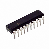
PIC16C770-I/P Microchip Technology, PIC16C770-I/P Datasheet - Page 59

PIC16C770-I/P
Manufacturer Part Number
PIC16C770-I/P
Description
IC MCU CMOS A/D 2K 20MHZ 20-DIP
Manufacturer
Microchip Technology
Series
PIC® 16Cr
Datasheets
1.PIC16C770-ISO.pdf
(220 pages)
2.PIC16C770-ISO.pdf
(6 pages)
3.PIC16C770-ISO.pdf
(8 pages)
Specifications of PIC16C770-I/P
Core Size
8-Bit
Program Memory Size
3.5KB (2K x 14)
Oscillator Type
Internal
Core Processor
PIC
Speed
20MHz
Connectivity
I²C, SPI
Peripherals
Brown-out Detect/Reset, POR, PWM, WDT
Number Of I /o
15
Program Memory Type
OTP
Ram Size
256 x 8
Voltage - Supply (vcc/vdd)
4 V ~ 5.5 V
Data Converters
A/D 6x12b
Operating Temperature
-40°C ~ 85°C
Package / Case
20-DIP (0.300", 7.62mm)
Controller Family/series
PIC16C
No. Of I/o's
16
Ram Memory Size
256Byte
Cpu Speed
20MHz
No. Of Timers
3
No. Of
RoHS Compliant
Core
PIC
Processor Series
PIC16C
Data Bus Width
8 bit
Maximum Clock Frequency
20 MHz
Data Ram Size
256 B
Data Rom Size
256 B
On-chip Adc
6 bit
Number Of Programmable I/os
16
Number Of Timers
3 bit
Operating Supply Voltage
2.5 V to 5.5 V
Mounting Style
Through Hole
Height
3.3 mm
Interface Type
I2C, SPI, SSP
Length
26.16 mm
Maximum Operating Temperature
+ 85 C
Minimum Operating Temperature
- 40 C
Supply Voltage (max)
5.5 V
Supply Voltage (min)
4 V
Width
6.35 mm
Lead Free Status / RoHS Status
Lead free / RoHS Compliant
For Use With
DVA16XP200 - ADAPTER ICE 20DIP/SOIC/SSOPAC164028 - MODULE SKT PROMATEII 20SOIC/DIP
Eeprom Size
-
Lead Free Status / Rohs Status
Details
Other names
PIC16C770I/P
- Current page: 59 of 220
- Download datasheet (4Mb)
8.3.2
The PWM duty cycle is specified by writing to the
CCPR1L register and to the CCP1CON<5:4> bits. Up
to 10-bit resolution is available. The CCPR1L contains
the eight MSbs and the CCP1CON<5:4> contains the
two LSbs. This 10-bit value is represented by
CCPR1L:CCP1CON<5:4>. The following equation is
used to calculate the PWM duty cycle in time:
CCPR1L and CCP1CON<5:4> can be written to at any
time, but the duty cycle value is not latched into
CCPR1H until after a match between PR2 and TMR2
occurs (i.e., the period is complete). In PWM mode,
CCPR1H is a read-only register.
The CCPR1H register and a 2-bit internal latch are
used to double buffer the PWM duty cycle. This double
buffering is essential for glitchless PWM operation.
When the CCPR1H and 2-bit latch match TMR2 con-
catenated with an internal 2-bit Q clock or 2 bits of the
TMR2 prescaler, the CCP1 pin is cleared.
Maximum PWM resolution (bits) for a given PWM fre-
quency:
8.3.3
The PWM1M1 bits in the CCP1CON register allows
one of the following configurations:
• Single output
• Half-Bridge output
• Full-Bridge output, Forward mode
• Full-Bridge output, Reverse mode
In the Single Output mode, the RB3/CCP1/P1A pin is
used as the PWM output. Since the CCP1 output is
multiplexed with the PORTB<3> data latch, the
TRISB<3> bit must be cleared to make the CCP1 pin
an output.
2002 Microchip Technology Inc.
Note:
PWM duty cycle
PWM DUTY CYCLE
If the PWM duty cycle value is longer than
the PWM period, the CCP1 pin will not be
cleared.
PWM OUTPUT CONFIGURATIONS
=
log
-----------------------------bits
= (CCPR1L:CCP1CON<5:4>) •
log
T
OSC
---------------
F
F
PWM
OSC
2
• (TMR2 prescale value)
FIGURE 8-4:
FIGURE 8-5:
In the Half-Bridge Output mode, two pins are used as
outputs. The RB3/CCP1/P1A pin has the PWM output
signal, while the RB5/SDO/P1B pin has the comple-
mentary PWM output signal. This mode can be used
for half-bridge applications, as shown on Figure 8-7, or
for full-bridge applications, where four power switches
are being modulated with two PWM signal.
Since the P1A and P1B outputs are multiplexed with
the PORTB<3> and PORTB<5> data latches, the
TRISB<3> and TRISB<5> bits must be cleared to con-
figure P1A and P1B as outputs.
In Half-Bridge Output mode, the programmable dead-
band delay can be used to prevent shoot-through cur-
rent in bridge power devices. See Section 8.3.5 for
more details of the deadband delay operations.
Note 1: At this time, the TMR2 register is equal to the PR2 register.
CCP1
PIC16C717/770/771
PIC16C717/770/771
PIC16C717/770/771
2: Output signal is shown as asserted high.
(2)
(1)
CCP1
Duty Cycle
CCP1
Period
SINGLE PWM OUTPUT
EXAMPLE OF SINGLE
OUTPUT APPLICATION
R
V+
O
A
D
L
(1)
C
DS41120B-page 57
Vout
Using PWM to
Drive a Power
Load
Using PWM as
a D/A Converter
Related parts for PIC16C770-I/P
Image
Part Number
Description
Manufacturer
Datasheet
Request
R

Part Number:
Description:
IC MCU OTP 8KX14 A/D PWM 44PLCC
Manufacturer:
Microchip Technology
Datasheet:

Part Number:
Description:
IC MCU OTP 8KX14 A/D PWM 44PLCC
Manufacturer:
Microchip Technology
Datasheet:

Part Number:
Description:
IC MCU OTP 8KX14 A/D PWM 44TQFP
Manufacturer:
Microchip Technology
Datasheet:

Part Number:
Description:
IC MCU OTP 8KX14 A/D PWM 44-MQFP
Manufacturer:
Microchip Technology
Datasheet:

Part Number:
Description:
IC MCU OTP 8KX14 A/D PWM 40DIP
Manufacturer:
Microchip Technology
Datasheet:

Part Number:
Description:
IC MCU OTP 8KX14 A/D PWM 44PLCC
Manufacturer:
Microchip Technology
Datasheet:

Part Number:
Description:
IC MCU OTP 8KX14 A/D PWM 40DIP
Manufacturer:
Microchip Technology
Datasheet:

Part Number:
Description:
IC MCU OTP 8KX14 A/D PWM 40DIP
Manufacturer:
Microchip Technology
Datasheet:

Part Number:
Description:
IC MCU OTP 8KX14 A/D PWM 40DIP
Manufacturer:
Microchip Technology
Datasheet:

Part Number:
Description:
IC MCU OTP 8KX14 A/D PWM 44PLCC
Manufacturer:
Microchip Technology
Datasheet:

Part Number:
Description:
IC MCU OTP 8KX14 A/D PWM 44PLCC
Manufacturer:
Microchip Technology
Datasheet:

Part Number:
Description:
IC MCU OTP 8KX14 A/D PWM 44-MQFP
Manufacturer:
Microchip Technology
Datasheet:

Part Number:
Description:
IC MCU OTP 8KX14 A/D PWM 40DIP
Manufacturer:
Microchip Technology
Datasheet:

Part Number:
Description:
IC MCU OTP 8KX14 A/D PWM 44-MQFP
Manufacturer:
Microchip Technology
Datasheet:

Part Number:
Description:
IC MCU OTP 8KX14 A/D PWM 40DIP
Manufacturer:
Microchip Technology
Datasheet:


