PIC18LF13K22-I/ML Microchip Technology, PIC18LF13K22-I/ML Datasheet - Page 43
PIC18LF13K22-I/ML
Manufacturer Part Number
PIC18LF13K22-I/ML
Description
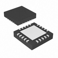
IC PIC MCU FLASH 256KX8 20-QFN
Manufacturer
Microchip Technology
Series
PIC® XLP™ 18Fr
Datasheets
1.PIC18LF13K22-ISS.pdf
(388 pages)
2.PIC18LF13K22-ISS.pdf
(12 pages)
3.PIC18LF13K22-ISS.pdf
(36 pages)
4.PIC18LF14K22-IP.pdf
(382 pages)
Specifications of PIC18LF13K22-I/ML
Program Memory Type
FLASH
Program Memory Size
8KB (4K x 16)
Package / Case
20-VQFN Exposed Pad, 20-HVQFN, 20-SQFN, 20-DHVQFN
Core Processor
PIC
Core Size
8-Bit
Speed
64MHz
Connectivity
I²C, LIN, SPI, UART/USART
Peripherals
Brown-out Detect/Reset, POR, PWM, WDT
Number Of I /o
17
Eeprom Size
256 x 8
Ram Size
256 x 8
Voltage - Supply (vcc/vdd)
1.8 V ~ 3.6 V
Data Converters
A/D 12x10b
Oscillator Type
Internal
Operating Temperature
-40°C ~ 85°C
Processor Series
PIC18LF
Core
PIC
Data Bus Width
8 bit
Data Ram Size
256 B
Interface Type
I2C, MSSP, SPI, USART
Maximum Clock Frequency
32 KHz
Number Of Programmable I/os
18
Number Of Timers
4
Operating Supply Voltage
1.8 V to 3.6 V
Maximum Operating Temperature
+ 125 C
Mounting Style
SMD/SMT
3rd Party Development Tools
52715-96, 52716-328, 52717-734, 52712-325, EWPIC18
Development Tools By Supplier
PG164130, DV164035, DV244005, DV164005
Minimum Operating Temperature
- 40 C
On-chip Adc
10 bit, 12 Channel
Lead Free Status / RoHS Status
Lead free / RoHS Compliant
Lead Free Status / RoHS Status
Lead free / RoHS Compliant, Lead free / RoHS Compliant
Available stocks
Company
Part Number
Manufacturer
Quantity
Price
Company:

Part Number:
PIC18LF13K22-I/ML
Manufacturer:
CAVIUM
Quantity:
155


3.4
While the program memory can be addressed in only
one way – through the program counter – information
in the data memory space can be addressed in several
ways. For most instructions, the addressing mode is
fixed. Other instructions may use up to three modes,
depending on which operands are used and whether or
not the extended instruction set is enabled.
The addressing modes are:
• Inherent
• Literal
• Direct
• Indirect
An additional addressing mode, Indexed Literal Offset,
is available when the extended instruction set is
enabled (XINST Configuration bit = 1). Its operation is
discussed in greater detail in Section 3.5.1 “Indexed
Addressing with Literal Offset”.
3.4.1
Many PIC18 control instructions do not need any argu-
ment at all; they either perform an operation that glob-
ally affects the device or they operate implicitly on one
register. This addressing mode is known as Inherent
Addressing. Examples include SLEEP, RESET and DAW.
Other instructions work in a similar way but require an
additional explicit argument in the opcode. This is
known as Literal Addressing mode because they
require some literal value as an argument. Examples
include ADDLW and MOVLW, which respectively, add or
move a literal value to the W register. Other examples
include CALL and GOTO, which include a 20-bit
program memory address.
3.4.2
Direct addressing specifies all or part of the source
and/or destination address of the operation within the
opcode itself. The options are specified by the
arguments accompanying the instruction.
In the core PIC18 instruction set, bit-oriented and byte-
oriented instructions use some version of direct
addressing by default. All of these instructions include
some 8-bit literal address as their Least Significant
Byte. This address specifies either a register address in
one of the banks of data RAM (Section 3.3.3 “General
Purpose Register File”) or a location in the Access
Bank (Section 3.3.2 “Access Bank”) as the data
source for the instruction.
2010 Microchip Technology Inc.
Note:
Data Addressing Modes
The execution of some instructions in the
core PIC18 instruction set are changed
when the PIC18 extended instruction set is
enabled. See Section 3.5 “Data Memory
and the Extended Instruction Set” for
more information.
INHERENT AND LITERAL
ADDRESSING
DIRECT ADDRESSING
Preliminary
PIC18F1XK22/LF1XK22
The Access RAM bit ‘a’ determines how the address is
interpreted. When ‘a’ is ‘1’, the contents of the BSR
(Section 3.3.1 “Bank Select Register (BSR)”) are
used with the address to determine the complete 12-bit
address of the register. When ‘a’ is ‘0’, the address is
interpreted as being a register in the Access Bank.
Addressing that uses the Access RAM is sometimes
also known as Direct Forced Addressing mode.
A few instructions, such as MOVFF, include the entire
12-bit address (either source or destination) in their
opcodes. In these cases, the BSR is ignored entirely.
The destination of the operation’s results is determined
by the destination bit ‘d’. When ‘d’ is ‘1’, the results are
stored back in the source register, overwriting its origi-
nal contents. When ‘d’ is ‘0’, the results are stored in
the W register. Instructions without the ‘d’ argument
have a destination that is implicit in the instruction; their
destination is either the target register being operated
on or the W register.
3.4.3
Indirect addressing allows the user to access a location
in data memory without giving a fixed address in the
instruction. This is done by using File Select Registers
(FSRs) as pointers to the locations which are to be read
or written. Since the FSRs are themselves located in
RAM as Special File Registers, they can also be
directly manipulated under program control. This
makes FSRs very useful in implementing data struc-
tures, such as tables and arrays in data memory.
The registers for indirect addressing are also
implemented with Indirect File Operands (INDFs) that
permit automatic manipulation of the pointer value with
auto-incrementing, auto-decrementing or offsetting
with another value. This allows for efficient code, using
loops, such as the example of clearing an entire RAM
bank in Example 3-5.
EXAMPLE 3-5:
NEXT
CONTINUE
LFSR
CLRF
BTFSS
BRA
INDIRECT ADDRESSING
FSR0, 100h ;
POSTINC0
FSR0H, 1
NEXT
HOW TO CLEAR RAM
(BANK 1) USING
INDIRECT ADDRESSING
; Clear INDF
; register then
; inc pointer
; All done with
; Bank1?
; NO, clear next
; YES, continue
DS41365D-page 43
Related parts for PIC18LF13K22-I/ML
Image
Part Number
Description
Manufacturer
Datasheet
Request
R

Part Number:
Description:
Manufacturer:
Microchip Technology Inc.
Datasheet:
Part Number:
Description:
Manufacturer:
Microchip Technology Inc.
Datasheet:
Part Number:
Description:
Manufacturer:
Microchip Technology Inc.
Datasheet:
Part Number:
Description:
Manufacturer:
Microchip Technology Inc.
Datasheet:
Part Number:
Description:
Manufacturer:
Microchip Technology Inc.
Datasheet:
Part Number:
Description:
Manufacturer:
Microchip Technology Inc.
Datasheet:
Part Number:
Description:
Manufacturer:
Microchip Technology Inc.
Datasheet:
Part Number:
Description:
Manufacturer:
Microchip Technology Inc.
Datasheet: