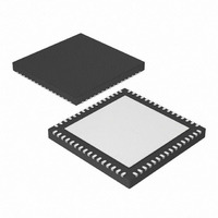
PIC24FJ128GA106-E/MR Microchip Technology, PIC24FJ128GA106-E/MR Datasheet - Page 231

PIC24FJ128GA106-E/MR
Manufacturer Part Number
PIC24FJ128GA106-E/MR
Description
IC PIC MCU FLASH 128K 64-QFN
Manufacturer
Microchip Technology
Series
PIC® 24Fr
Datasheets
1.PIC24FJ128GA106-IPT.pdf
(14 pages)
2.PIC24FJ128GA106-IPT.pdf
(330 pages)
3.PIC24FJ128GA106-IPT.pdf
(52 pages)
4.PIC24FJ128GA110-EPT.pdf
(310 pages)
Specifications of PIC24FJ128GA106-E/MR
Program Memory Type
FLASH
Program Memory Size
128KB (43K x 24)
Package / Case
64-VFQFN, Exposed Pad
Core Processor
PIC
Core Size
16-Bit
Speed
32MHz
Connectivity
I²C, PMP, SPI, UART/USART
Peripherals
Brown-out Detect/Reset, POR, PWM, WDT
Number Of I /o
53
Ram Size
16K x 8
Voltage - Supply (vcc/vdd)
2 V ~ 3.6 V
Data Converters
A/D 16x10b
Oscillator Type
Internal
Operating Temperature
-40°C ~ 125°C
Processor Series
PIC24FJ
Core
PIC
Data Bus Width
16 bit
Data Ram Size
16 KB
Interface Type
I2C/SPI/UART
Maximum Clock Frequency
32 MHz
Number Of Programmable I/os
53
Number Of Timers
5
Maximum Operating Temperature
+ 125 C
Mounting Style
SMD/SMT
3rd Party Development Tools
52713-733, 52714-737, 53276-922, EWDSPIC
Development Tools By Supplier
PG164130, DV164035, DV244005, DV164005, PG164120, DM240001
Minimum Operating Temperature
- 40 C
On-chip Adc
16-ch x 10-bit
Lead Free Status / RoHS Status
Lead free / RoHS Compliant
Eeprom Size
-
Lead Free Status / Rohs Status
Lead free / RoHS Compliant
- PIC24FJ128GA106-IPT PDF datasheet
- PIC24FJ128GA106-IPT PDF datasheet #2
- PIC24FJ128GA106-IPT PDF datasheet #3
- PIC24FJ128GA110-EPT PDF datasheet #4
- Current page: 231 of 330
- Download datasheet (3Mb)
REGISTER 21-5:
REGISTER 21-6:
2010 Microchip Technology Inc.
bit 15
bit 7
Legend:
R = Readable bit
-n = Value at POR
bit 15-0
bit 15
bit 7
Legend:
R = Readable bit
-n = Value at POR
bit 15-2
bit 1
bit 0
PCFG15
PCFG7
R/W-0
R/W-0
U-0
U-0
—
—
PCFG<15:0>: Analog Input Pin Configuration Control bits
1 = Pin for corresponding analog channel is configured in Digital mode; I/O port read enabled
0 = Pin configured in Analog mode; I/O port read disabled, A/D samples pin voltage
Unimplemented: Read as ‘0’
PCFG17: A/D Input Band Gap Scan Enable bit
1 = Analog channel disabled from input scan
0 = Internal band gap (V
PCFG16: A/D Input Half Band Gap Scan Enable bit
1 = Analog channel disabled from input scan
0 = Internal V
PCFG14
PCFG6
R/W-0
R/W-0
U-0
U-0
—
—
AD1PCFGL: A/D PORT CONFIGURATION REGISTER (LOW)
AD1PCFGH: A/D PORT CONFIGURATION REGISTER (HIGH)
BG
W = Writable bit
‘1’ = Bit is set
W = Writable bit
‘1’ = Bit is set
/2 channel enabled for input scan
PCFG13
PCFG5
R/W-0
R/W-0
U-0
U-0
—
—
BG
) channel enabled for input scan
PCFG12
PIC24FJ256GA110 FAMILY
PCFG4
R/W-0
R/W-0
U-0
U-0
—
—
U = Unimplemented bit, read as ‘0’
‘0’ = Bit is cleared
U = Unimplemented bit, read as ‘0’
‘0’ = Bit is cleared
PCFG11
PCFG3
R/W-0
R/W-0
U-0
U-0
—
—
PCFG10
PCFG2
R/W-0
R/W-0
U-0
U-0
—
—
x = Bit is unknown
x = Bit is unknown
PCFG17
PCFG9
PCFG1
R/W-0
R/W-0
R/W-0
U-0
—
DS39905E-page 231
PCFG16
PCFG0
PCFG8
R/W-0
R/W-0
R/W-0
U-0
—
bit 8
bit 0
bit 8
bit 0
Related parts for PIC24FJ128GA106-E/MR
Image
Part Number
Description
Manufacturer
Datasheet
Request
R

Part Number:
Description:
General Purpose, 16-Bit Flash Microcontrollers
Manufacturer:
MICROCHIP [Microchip Technology]
Datasheet:

Part Number:
Description:
Manufacturer:
Microchip Technology Inc.
Datasheet:

Part Number:
Description:
Manufacturer:
Microchip Technology Inc.
Datasheet:

Part Number:
Description:
Manufacturer:
Microchip Technology Inc.
Datasheet:

Part Number:
Description:
Manufacturer:
Microchip Technology Inc.
Datasheet:

Part Number:
Description:
Manufacturer:
Microchip Technology Inc.
Datasheet:

Part Number:
Description:
Manufacturer:
Microchip Technology Inc.
Datasheet:

Part Number:
Description:
Manufacturer:
Microchip Technology Inc.
Datasheet:

Part Number:
Description:
Manufacturer:
Microchip Technology Inc.
Datasheet:


