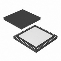
PIC24FJ128GA106-E/MR Microchip Technology, PIC24FJ128GA106-E/MR Datasheet - Page 48

PIC24FJ128GA106-E/MR
Manufacturer Part Number
PIC24FJ128GA106-E/MR
Description
IC PIC MCU FLASH 128K 64-QFN
Manufacturer
Microchip Technology
Series
PIC® 24Fr
Datasheets
1.PIC24FJ128GA106-IPT.pdf
(14 pages)
2.PIC24FJ128GA106-IPT.pdf
(330 pages)
3.PIC24FJ128GA106-IPT.pdf
(52 pages)
4.PIC24FJ128GA110-EPT.pdf
(310 pages)
Specifications of PIC24FJ128GA106-E/MR
Program Memory Type
FLASH
Program Memory Size
128KB (43K x 24)
Package / Case
64-VFQFN, Exposed Pad
Core Processor
PIC
Core Size
16-Bit
Speed
32MHz
Connectivity
I²C, PMP, SPI, UART/USART
Peripherals
Brown-out Detect/Reset, POR, PWM, WDT
Number Of I /o
53
Ram Size
16K x 8
Voltage - Supply (vcc/vdd)
2 V ~ 3.6 V
Data Converters
A/D 16x10b
Oscillator Type
Internal
Operating Temperature
-40°C ~ 125°C
Processor Series
PIC24FJ
Core
PIC
Data Bus Width
16 bit
Data Ram Size
16 KB
Interface Type
I2C/SPI/UART
Maximum Clock Frequency
32 MHz
Number Of Programmable I/os
53
Number Of Timers
5
Maximum Operating Temperature
+ 125 C
Mounting Style
SMD/SMT
3rd Party Development Tools
52713-733, 52714-737, 53276-922, EWDSPIC
Development Tools By Supplier
PG164130, DV164035, DV244005, DV164005, PG164120, DM240001
Minimum Operating Temperature
- 40 C
On-chip Adc
16-ch x 10-bit
Lead Free Status / RoHS Status
Lead free / RoHS Compliant
Eeprom Size
-
Lead Free Status / Rohs Status
Lead free / RoHS Compliant
- PIC24FJ128GA106-IPT PDF datasheet
- PIC24FJ128GA106-IPT PDF datasheet #2
- PIC24FJ128GA106-IPT PDF datasheet #3
- PIC24FJ128GA110-EPT PDF datasheet #4
- Current page: 48 of 330
- Download datasheet (3Mb)
TABLE 4-16:
TABLE 4-17:
TABLE 4-18:
TABLE 4-19:
TRISE
PORTE
LATE
ODCE
Legend:
Note 1:
TRISF
PORTF
LATF
ODCF
Legend:
Note
TRISG
PORTG
LATG
ODCG
Legend:
Note
PADCFG1 02FC
Legend:
Name
Name
Name
Name
File
File
File
File
1:
2:
1:
2:
Addr
02E0
02E2
02E4
02E6
Addr
02E8
02EA
02EC
02EE
Addr
02F0
02F2
02F4
02F6
Addr
— = unimplemented, read as ‘0’. Reset values are shown in hexadecimal. Reset values shown are for 100-pin devices.
Bits are unimplemented in 64-pin devices; read as ‘0’.
— = unimplemented, read as ‘0’. Reset values are shown in hexadecimal. Reset values shown are for 100-pin devices.
Bits are unimplemented in 64-pin and 80-pin devices; read as ‘0’.
Bits are unimplemented in 64-pin devices; read as ‘0’.
— = unimplemented, read as ‘0’. Reset values are shown in hexadecimal. Reset values shown are for 100-pin devices.
Bits unimplemented in 64-pin and 80-pin devices; read as ‘0’.
Bits unimplemented in 64-pin devices; read as ‘0’.
— = unimplemented, read as ‘0’. Reset values are shown in hexadecimal.
TRISG15 TRISG14 TRISG13 TRISG12
Bit 15
LATG15
ODG15
Bit 15
Bit 15
RG15
Bit 15
PORTE REGISTER MAP
PORTF REGISTER MAP
PORTG REGISTER MAP
PAD CONFIGURATION REGISTER MAP
—
—
—
—
—
—
—
—
—
(1)
Bit 14
LATG14
ODG14
Bit 14
Bit 14
RG14
Bit 14
—
—
—
—
—
—
—
—
—
(1)
TRISF13 TRISF12
Bit 13
Bit 13
LATG13
LATF13
ODG13
ODF13
Bit 13
Bit 13
RG13
RF13
—
—
—
—
—
(1)
(1)
Bit 12
Bit 12
LATG12
LATF12
Bit 12
ODF12
ODG12
Bit 12
RG12
RF12
—
—
—
—
—
(1)
(1)
Bit 11
Bit 11
Bit 11
Bit 11
—
—
—
—
—
—
—
—
—
—
—
—
—
Bit 10
Bit 10
Bit 10
Bit 10
—
—
—
—
—
—
—
—
—
—
—
—
—
Bit 9
TRISE9
TRISG9
Bit 9
LATG9
LATE9
ODG9
—
ODE9
Bit 9
Bit 9
RE9
RG9
—
—
—
—
(1)
Bit 8
TRISE8
TRISG8
TRISF8
—
Bit 8
Bit 8
LATG8
LATE8
LATF8
ODG8
ODE8
ODF8
Bit 8
RE8
RG8
RF8
(2)
(1)
Bit 7
TRISE7
TRISG7
—
TRISF7
Bit 7
LATG7
LATE7
LATF7
ODG7
ODE7
ODF7
Bit 7
Bit 7
RE7
RG7
RF7
(2)
Bit 6
TRISE6
TRISG6
—
TRISF6
LATG6
LATE6
LATF6
ODG6
ODE6
ODF6
Bit 6
Bit 6
Bit 6
RE6
RG6
RF6
Bit 5
—
TRISE5
TRISF5
LATE5
LATF5
ODE5
ODF5
Bit 5
Bit 5
RE5
Bit 5
RF5
—
—
—
—
Bit 4
—
TRISE4
TRISF4
LATE4
LATF4
ODE4
ODF4
Bit 4
Bit 4
RE4
Bit 4
RF4
—
—
—
—
Bit 3
—
TRISG3
TRISE3
TRISF3
LATG3
LATE3
LATF3
ODE3
ODF3
ODG3
Bit 3
RE3
Bit 3
Bit 3
RG3
RF3
Bit 2
—
TRISG2
TRISE2
TRISF2
LATG2
LATE2
LATF2
ODE2
ODF2
ODG2
Bit 2
Bit 2
Bit 2
RG2
RE2
RF2
RTSECSEL
Bit 1
TRISG1
TRISE1
TRISF1
Bit 1
LATG1
LATE1
LATF1
ODE1
ODF1
ODG1
Bit 1
Bit 1
RG1
RE1
RF1
(2)
PMPTTL
TRISG0
TRISE0
TRISF0
Bit 0
LATE0
LATF0
LATG0
ODE0
ODF0
ODG0
Bit 0
Bit 0
Bit 0
RG0
RE0
RF0
(2)
Resets
Resets
Resets
Resets
F3CF
xxxx
xxxx
0000
03FF
xxxx
xxxx
0000
0000
31FF
xxxx
xxxx
0000
All
All
All
All
Related parts for PIC24FJ128GA106-E/MR
Image
Part Number
Description
Manufacturer
Datasheet
Request
R

Part Number:
Description:
General Purpose, 16-Bit Flash Microcontrollers
Manufacturer:
MICROCHIP [Microchip Technology]
Datasheet:

Part Number:
Description:
Manufacturer:
Microchip Technology Inc.
Datasheet:

Part Number:
Description:
Manufacturer:
Microchip Technology Inc.
Datasheet:

Part Number:
Description:
Manufacturer:
Microchip Technology Inc.
Datasheet:

Part Number:
Description:
Manufacturer:
Microchip Technology Inc.
Datasheet:

Part Number:
Description:
Manufacturer:
Microchip Technology Inc.
Datasheet:

Part Number:
Description:
Manufacturer:
Microchip Technology Inc.
Datasheet:

Part Number:
Description:
Manufacturer:
Microchip Technology Inc.
Datasheet:

Part Number:
Description:
Manufacturer:
Microchip Technology Inc.
Datasheet:


