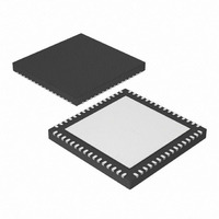
PIC24FJ128GA106-E/MR Microchip Technology, PIC24FJ128GA106-E/MR Datasheet - Page 177

PIC24FJ128GA106-E/MR
Manufacturer Part Number
PIC24FJ128GA106-E/MR
Description
IC PIC MCU FLASH 128K 64-QFN
Manufacturer
Microchip Technology
Series
PIC® 24Fr
Datasheets
1.PIC24FJ128GA106-IPT.pdf
(14 pages)
2.PIC24FJ128GA106-IPT.pdf
(330 pages)
3.PIC24FJ128GA106-IPT.pdf
(52 pages)
4.PIC24FJ128GA110-EPT.pdf
(310 pages)
Specifications of PIC24FJ128GA106-E/MR
Program Memory Type
FLASH
Program Memory Size
128KB (43K x 24)
Package / Case
64-VFQFN, Exposed Pad
Core Processor
PIC
Core Size
16-Bit
Speed
32MHz
Connectivity
I²C, PMP, SPI, UART/USART
Peripherals
Brown-out Detect/Reset, POR, PWM, WDT
Number Of I /o
53
Ram Size
16K x 8
Voltage - Supply (vcc/vdd)
2 V ~ 3.6 V
Data Converters
A/D 16x10b
Oscillator Type
Internal
Operating Temperature
-40°C ~ 125°C
Processor Series
PIC24FJ
Core
PIC
Data Bus Width
16 bit
Data Ram Size
16 KB
Interface Type
I2C/SPI/UART
Maximum Clock Frequency
32 MHz
Number Of Programmable I/os
53
Number Of Timers
5
Maximum Operating Temperature
+ 125 C
Mounting Style
SMD/SMT
3rd Party Development Tools
52713-733, 52714-737, 53276-922, EWDSPIC
Development Tools By Supplier
PG164130, DV164035, DV244005, DV164005, PG164120, DM240001
Minimum Operating Temperature
- 40 C
On-chip Adc
16-ch x 10-bit
Lead Free Status / RoHS Status
Lead free / RoHS Compliant
Eeprom Size
-
Lead Free Status / Rohs Status
Lead free / RoHS Compliant
- PIC24FJ128GA106-IPT PDF datasheet
- PIC24FJ128GA106-IPT PDF datasheet #2
- PIC24FJ128GA106-IPT PDF datasheet #3
- PIC24FJ128GA110-EPT PDF datasheet #4
- Current page: 177 of 310
- Download datasheet (3Mb)
To set up the SPI module for the Enhanced Buffer
Master mode of operation:
1.
2.
3.
4.
5.
6.
FIGURE 15-2:
2009 Microchip Technology Inc.
SSx/FSYNCx
If using interrupts:
a)
b)
c)
Write the desired settings to the SPIxCON1 and
SPIxCON2 registers with the MSTEN bit
(SPIxCON1<5>) = 1.
Clear the SPIROV bit (SPIxSTAT<6>).
Select Enhanced Buffer mode by setting the
SPIBEN bit (SPIxCON2<0>).
Enable SPI operation by setting the SPIEN bit
(SPIxSTAT<15>).
Write the data to be transmitted to the SPIxBUF
register. Transmission (and reception) will start
as soon as data is written to the SPIxBUF
register.
SDOx
SCKx
SDIx
Clear the SPIxIF bit in the respective IFSx
register.
Set the SPIxIE bit in the respective IECx
register.
Write the SPIxIP bits in the respective IPCx
register.
Read SPIxBUF
Control
Transfer
Sync
SPIx MODULE BLOCK DIAGRAM (ENHANCED MODE)
Receive Buffer
8-Level FIFO
bit0
SPIxSR
Control
SPIxBUF
Clock
Shift Control
Transmit Buffer
8-Level FIFO
PIC24FJ256GA110 FAMILY
Transfer
Write SPIxBUF
Select
Edge
To set up the SPI module for the Enhanced Buffer
Slave mode of operation:
1.
2.
3.
4.
5.
6.
7.
8.
16
Clear the SPIxBUF register.
If using interrupts:
a)
b)
c)
Write the desired settings to the SPIxCON1 and
SPIxCON2 registers with the MSTEN bit
(SPIxCON1<5>) = 0.
Clear the SMP bit.
If the CKE bit is set, then the SSEN bit must be
set, thus enabling the SSx pin.
Clear the SPIROV bit (SPIxSTAT<6>).
Select Enhanced Buffer mode by setting the
SPIBEN bit (SPIxCON2<0>).
Enable SPI operation by setting the SPIEN bit
(SPIxSTAT<15>).
Secondary
Clear the SPIxIF bit in the respective IFSx
register.
Set the SPIxIE bit in the respective IECx
register.
Write the SPIxIP bits in the respective IPCx
register to set the interrupt priority.
Prescaler
1:1 to 1:8
Internal Data Bus
1:1/4/16/64
Prescaler
Primary
DS39905D-page 177
SPIxCON1<1:0>
SPIxCON1<4:2>
Enable
Master Clock
F
CY
Related parts for PIC24FJ128GA106-E/MR
Image
Part Number
Description
Manufacturer
Datasheet
Request
R

Part Number:
Description:
General Purpose, 16-Bit Flash Microcontrollers
Manufacturer:
MICROCHIP [Microchip Technology]
Datasheet:

Part Number:
Description:
Manufacturer:
Microchip Technology Inc.
Datasheet:

Part Number:
Description:
Manufacturer:
Microchip Technology Inc.
Datasheet:

Part Number:
Description:
Manufacturer:
Microchip Technology Inc.
Datasheet:

Part Number:
Description:
Manufacturer:
Microchip Technology Inc.
Datasheet:

Part Number:
Description:
Manufacturer:
Microchip Technology Inc.
Datasheet:

Part Number:
Description:
Manufacturer:
Microchip Technology Inc.
Datasheet:

Part Number:
Description:
Manufacturer:
Microchip Technology Inc.
Datasheet:

Part Number:
Description:
Manufacturer:
Microchip Technology Inc.
Datasheet:


