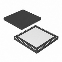
PIC24FJ128GA106-E/MR Microchip Technology, PIC24FJ128GA106-E/MR Datasheet - Page 222

PIC24FJ128GA106-E/MR
Manufacturer Part Number
PIC24FJ128GA106-E/MR
Description
IC PIC MCU FLASH 128K 64-QFN
Manufacturer
Microchip Technology
Series
PIC® 24Fr
Datasheets
1.PIC24FJ128GA106-IPT.pdf
(14 pages)
2.PIC24FJ128GA106-IPT.pdf
(330 pages)
3.PIC24FJ128GA106-IPT.pdf
(52 pages)
4.PIC24FJ128GA110-EPT.pdf
(310 pages)
Specifications of PIC24FJ128GA106-E/MR
Program Memory Type
FLASH
Program Memory Size
128KB (43K x 24)
Package / Case
64-VFQFN, Exposed Pad
Core Processor
PIC
Core Size
16-Bit
Speed
32MHz
Connectivity
I²C, PMP, SPI, UART/USART
Peripherals
Brown-out Detect/Reset, POR, PWM, WDT
Number Of I /o
53
Ram Size
16K x 8
Voltage - Supply (vcc/vdd)
2 V ~ 3.6 V
Data Converters
A/D 16x10b
Oscillator Type
Internal
Operating Temperature
-40°C ~ 125°C
Processor Series
PIC24FJ
Core
PIC
Data Bus Width
16 bit
Data Ram Size
16 KB
Interface Type
I2C/SPI/UART
Maximum Clock Frequency
32 MHz
Number Of Programmable I/os
53
Number Of Timers
5
Maximum Operating Temperature
+ 125 C
Mounting Style
SMD/SMT
3rd Party Development Tools
52713-733, 52714-737, 53276-922, EWDSPIC
Development Tools By Supplier
PG164130, DV164035, DV244005, DV164005, PG164120, DM240001
Minimum Operating Temperature
- 40 C
On-chip Adc
16-ch x 10-bit
Lead Free Status / RoHS Status
Lead free / RoHS Compliant
Eeprom Size
-
Lead Free Status / Rohs Status
Lead free / RoHS Compliant
- PIC24FJ128GA106-IPT PDF datasheet
- PIC24FJ128GA106-IPT PDF datasheet #2
- PIC24FJ128GA106-IPT PDF datasheet #3
- PIC24FJ128GA110-EPT PDF datasheet #4
- Current page: 222 of 310
- Download datasheet (3Mb)
PIC24FJ256GA110 FAMILY
FIGURE 20-2:
20.1
20.1.1
To start serial shifting, a ‘1’ must be written to the
CRCGO bit.
The module incorporates a FIFO that is 8 deep when
PLEN<3:0> (CRCCON<3:0>) > 7 and 16 deep, other-
wise. The data for which the CRC is to be calculated
must first be written into the FIFO. The smallest data
element that can be written into the FIFO is one byte.
For example, if PLEN = 5, then the size of the data is
PLEN + 1 = 6. When loading data, the two MSbs of the
data byte are ignored.
Once data is written into the CRCWDAT MSb (as
defined by PLEN), the value of VWORD<4:0>
(CRCCON<12:8>)
CRCGO = 1 and VWORD > 0, a word of data to be
shifted is moved from the FIFO into the shift engine.
When the data word moves from the FIFO to the shift
engine, the VWORD bits decrement by one. The serial
shifter continues to receive data from the FIFO, shifting
until the VWORD bits reach 0. The last bit of data will
be shifted through the CRC module (PLEN + 1)/2 clock
cycles after the VWORD bits reach 0. This is when the
module is completed with the CRC calculation.
Therefore, for a given value of PLEN, it will take
(PLEN + 1)/2 * VWORD number of clock cycles to
complete the CRC calculations.
When VWORD<4:0> reach 8 (or 16), the CRCFUL bit
will be set. When VWORD<4:0> reach 0, the CRCMPT
bit will be set.
To continually feed data into the CRC engine, the
recommended mode of operation is to initially “prime”
the FIFO with a sufficient number of words so no inter-
rupt is generated before the next word can be written.
Once that is done, start the CRC by setting the CRCGO
bit to ‘1’. From that point onward, the VWORD bits
should be polled. If they read less than 8 or 16, another
word can be written into the FIFO.
DS39905D-page 222
Note 1: Each XOR stage of the shift engine is programmable. See text for details.
Shift Buffer
Data
User Interface
2: Polynomial length n is determined by ([PLEN<3:0>] + 1).
DATA INTERFACE
increments
CRC SHIFT ENGINE DETAIL
Bit 0
Read/Write Bus
by
one.
X(1)
(1)
When
Bit 1
To empty words already written into a FIFO, the
CRCGO bit must be set to ‘1’ and the CRC shifter
allowed to run until the CRCMPT bit is set.
Also, to get the correct CRC reading, it will be
necessary to wait for the CRCMPT bit to go high before
reading the CRCWDAT register.
If a word is written when the CRCFUL bit is set, the
VWORD Pointer will roll over to 0. The hardware will
then behave as if the FIFO is empty. However, the con-
dition to generate an interrupt will not be met; therefore,
no interrupt will be generated (See Section 20.1.2
“Interrupt Operation”).
At least one instruction cycle must pass after a write to
CRCWDAT before a read of the VWORD bits is done.
20.1.2
When the VWORD<4:0> bits make a transition from a
value of ‘1’ to ‘0’, an interrupt will be generated. Note
that the CRC calculation is not complete at this point;
an additional time of (PLEN + 1)/2 clock cycles is
required before the output can be read.
20.2
20.2.1
If Sleep mode is entered while the module is operating,
the module will be suspended in its current state until
clock execution resumes.
20.2.2
To continue full module operation in Idle mode, the
CSIDL bit must be cleared prior to entry into the mode.
If CSIDL = 1, the module will behave the same way as
it does in Sleep mode; pending interrupt events will be
passed on, even though the module clocks are not
available.
X(2)
CRCWDAT
(1)
Operation in Power Save Modes
Bit 2
INTERRUPT OPERATION
SLEEP MODE
IDLE MODE
2009 Microchip Technology Inc.
X(n)
(1)
Bit n
(2)
Related parts for PIC24FJ128GA106-E/MR
Image
Part Number
Description
Manufacturer
Datasheet
Request
R

Part Number:
Description:
General Purpose, 16-Bit Flash Microcontrollers
Manufacturer:
MICROCHIP [Microchip Technology]
Datasheet:

Part Number:
Description:
Manufacturer:
Microchip Technology Inc.
Datasheet:

Part Number:
Description:
Manufacturer:
Microchip Technology Inc.
Datasheet:

Part Number:
Description:
Manufacturer:
Microchip Technology Inc.
Datasheet:

Part Number:
Description:
Manufacturer:
Microchip Technology Inc.
Datasheet:

Part Number:
Description:
Manufacturer:
Microchip Technology Inc.
Datasheet:

Part Number:
Description:
Manufacturer:
Microchip Technology Inc.
Datasheet:

Part Number:
Description:
Manufacturer:
Microchip Technology Inc.
Datasheet:

Part Number:
Description:
Manufacturer:
Microchip Technology Inc.
Datasheet:


