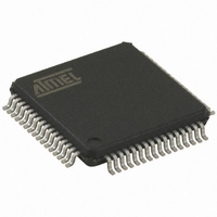
AT89C5130A-RDRUM Atmel, AT89C5130A-RDRUM Datasheet - Page 107

AT89C5130A-RDRUM
Manufacturer Part Number
AT89C5130A-RDRUM
Description
MCU 8051 16K FLASH USB 64-VQFP
Manufacturer
Atmel
Series
AT89C513xr
Datasheet
1.AT89C5130A-PUTUM.pdf
(188 pages)
Specifications of AT89C5130A-RDRUM
Core Processor
C52X2
Core Size
8-Bit
Speed
48MHz
Connectivity
I²C, SPI, UART/USART, USB
Peripherals
LED, POR, PWM, WDT
Number Of I /o
34
Program Memory Size
16KB (16K x 8)
Program Memory Type
FLASH
Eeprom Size
4K x 8
Ram Size
1.25K x 8
Voltage - Supply (vcc/vdd)
2.7 V ~ 5.5 V
Oscillator Type
Internal
Operating Temperature
-40°C ~ 85°C
Package / Case
64-TQFP, 64-VQFP
Processor Series
AT89x
Core
8051
Data Bus Width
8 bit
Mounting Style
SMD/SMT
3rd Party Development Tools
PK51, CA51, A51, ULINK2
Development Tools By Supplier
AT89STK-05
Lead Free Status / RoHS Status
Lead free / RoHS Compliant
Data Converters
-
Available stocks
Company
Part Number
Manufacturer
Quantity
Price
- Current page: 107 of 188
- Download datasheet (2Mb)
20.1.4
20.1.5
20.2
4337K–USB–04/08
CR2
0
0
0
0
Notes
Slave Transmitter Mode
Miscellaneous States
CR1
0
0
1
1
CR0
0
1
0
1
In the slave transmitter mode, a number of data bytes are transmitted to a master receiver
(Figure 20-7). Data transfer is initialized as in the slave receiver mode. When SSADR and
SSCON have been initialized, the TWI module waits until it is addressed by its own slave
address followed by the data direction bit which must be at logic 1 (R) for TWI to operate in the
slave transmitter mode. After its own slave address and the R bit have been received, the serial
interrupt flag is set and a valid status code can be read from SSCS. This status code is used to
vector to an interrupt service routine. The appropriate action to be taken for each of these status
code is detailed in Table . The slave transmitter mode may also be entered if arbitration is lost
while the TWI module is in the master mode.
If the AA bit is reset during a transfer, the TWI module will transmit the last byte of the transfer
and enter state C0h or C8h. the TWI module is switched to the not addressed slave mode and
will ignore the master receiver if it continues the transfer. Thus the master receiver receives all
1’s as serial data. While AA is reset, the TWI module does not respond to its own slave address.
However, the 2-wire bus is still monitored and address recognition may be resume at any time
by setting AA. This means that the AA bit may be used to temporarily isolate the TWI module
from the 2-wire bus.
There are two SSCS codes that do not correspond to a define TWI hardware state (Table 20-9 ).
These codes are discuss hereafter.
Status F8h indicates that no relevant information is available because the serial interrupt flag is
not set yet. This occurs between other states and when the TWI module is not involved in a
serial transfer.
Status 00h indicates that a bus error has occurred during a TWI serial transfer. A bus error is
caused when a START or a STOP condition occurs at an illegal position in the format frame.
Examples of such illegal positions happen during the serial transfer of an address byte, a data
byte, or an acknowledge bit. When a bus error occurs, SI is set. To recover from a bus error, the
STO flag must be set and SI must be cleared. This causes the TWI module to enter the not
addressed slave mode and to clear the STO flag (no other bits in SSCON are affected). The
SDA and SCL lines are released and no STOP condition is transmitted.
The TWI module interfaces to the external 2-wire bus via two port pins: SCL (serial clock line)
and SDA (serial data line). To avoid low level asserting on these lines when the TWI module is
enabled, the output latches of SDA and SLC must be set to logic 1.
Table 20-4.
F
OSCA
53.5
62.5
= 12 MHz
Bit Frequency Configuration
47
75
Bit Frequency ( kHz)
F
OSCA
62.5
71.5
100
= 16 MHz
83
AT89C5130A/31A-M
F
OSCA
divided by
256
224
192
160
107
Related parts for AT89C5130A-RDRUM
Image
Part Number
Description
Manufacturer
Datasheet
Request
R

Part Number:
Description:
Manufacturer:
Atmel Corporation
Datasheet:

Part Number:
Description:
IC 8051 MCU FLASH 16K USB 32QFN
Manufacturer:
Atmel
Datasheet:

Part Number:
Description:
IC 8051 MCU FLASH 16K USB 52PLCC
Manufacturer:
Atmel
Datasheet:

Part Number:
Description:
IC 8051 MCU FLASH 16K USB 64VQFP
Manufacturer:
Atmel
Datasheet:

Part Number:
Description:
IC 8051 MCU FLASH 16K USB 64VQFP
Manufacturer:
Atmel
Datasheet:

Part Number:
Description:
8-bit Microcontrollers - MCU Microcontroller
Manufacturer:
Atmel

Part Number:
Description:
IC MICRO CTRL 24MHZ 44TQFP
Manufacturer:
Atmel
Datasheet:

Part Number:
Description:
IC MICRO CTRL 24MHZ 44PLCC
Manufacturer:
Atmel
Datasheet:

Part Number:
Description:
IC MICRO CTRL 24MHZ 44PLCC
Manufacturer:
Atmel
Datasheet:

Part Number:
Description:
IC MICRO CTRL 24MHZ 40DIP
Manufacturer:
Atmel
Datasheet:

Part Number:
Description:
IC MICRO CTRL 24MHZ 40DIP
Manufacturer:
Atmel
Datasheet:

Part Number:
Description:
8-bit microcontroller with 4K bytes flash, 5V, 20MHz
Manufacturer:
ATMEL Corporation
Datasheet:

Part Number:
Description:
8-bit microcontroller with 4K bytes flash, 5V, 20MHz
Manufacturer:
ATMEL Corporation
Datasheet:


