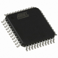
AT89C51CC01UA-RLRUM Atmel, AT89C51CC01UA-RLRUM Datasheet - Page 37

AT89C51CC01UA-RLRUM
Manufacturer Part Number
AT89C51CC01UA-RLRUM
Description
IC 8051 MCU 32K FLASH 44-VQFP
Manufacturer
Atmel
Series
AT89C CANr
Datasheet
1.T89C51CC01CA-7CTIM.pdf
(167 pages)
Specifications of AT89C51CC01UA-RLRUM
Core Processor
8051
Core Size
8-Bit
Speed
40MHz
Connectivity
CAN, UART/USART
Peripherals
POR, PWM, WDT
Number Of I /o
34
Program Memory Size
32KB (32K x 8)
Program Memory Type
FLASH
Eeprom Size
2K x 8
Ram Size
1.25K x 8
Voltage - Supply (vcc/vdd)
3 V ~ 5.5 V
Data Converters
A/D 8x10b
Oscillator Type
External
Operating Temperature
-40°C ~ 85°C
Package / Case
44-TQFP, 44-VQFP
Processor Series
AT89x
Core
8051
Data Bus Width
8 bit
Data Ram Size
1280 B
Interface Type
UART
Maximum Clock Frequency
40 MHz
Number Of Programmable I/os
34
Number Of Timers
2
Operating Supply Voltage
3 V to 5.5 V
Mounting Style
SMD/SMT
3rd Party Development Tools
PK51, CA51, A51, ULINK2
Development Tools By Supplier
CANADAPT28
For Use With
AT89OCD-01 - USB EMULATOR FOR AT8XC51 MCU
Lead Free Status / RoHS Status
Lead free / RoHS Compliant
Other names
AT89C51CC01UA-RLRUMTR
Available stocks
Company
Part Number
Manufacturer
Quantity
Price
- Current page: 37 of 167
- Download datasheet (2Mb)
Overview of FM0
Operations
Mapping of the Memory Space By default, the user space is accessed by MOVC instruction for read only. The column
Launching Programming
4129N–CAN–03/08
The CPU interfaces to the Flash memory through the FCON register and AUXR1
register.
These registers are used to:
•
•
•
latches space is made accessible by setting the FPS bit in FCON register. Writing is
possible from 0000h to 7FFFh, address bits 6 to 0 are used to select an address within a
page while bits 14 to 7 are used to select the programming address of the page.
Setting FPS bit takes precedence on the EXTRAM bit in AUXR register.
The other memory spaces (user, extra row, hardware security) are made accessible in
the code segment by programming bits FMOD0 and FMOD1 in FCON register in accor-
dance with Table 25. A MOVC instruction is then used for reading these spaces.
Table 25. FM0 Blocks Select Bits
FPL3:0 bits in FCON register are used to secure the launch of programming. A specific
sequence must be written in these bits to unlock the write protection and to launch the
programming. This sequence is 5xh followed by Axh. Table 26 summarizes the memory
spaces to program according to FMOD1:0 bits.
Map the memory spaces in the adressable space
Launch the programming of the memory spaces
Get the status of the Flash memory (busy/not busy)
FMOD1
0
0
1
1
FMOD0
0
1
0
1
FM0 Adressable space
User (0000h-7FFFh)
Extra Row(FF80h-FFFFh)
Hardware Security Byte (0000h)
Reserved
37
Related parts for AT89C51CC01UA-RLRUM
Image
Part Number
Description
Manufacturer
Datasheet
Request
R

Part Number:
Description:
Manufacturer:
Atmel Corporation
Datasheet:

Part Number:
Description:
DEV KIT FOR AVR/AVR32
Manufacturer:
Atmel
Datasheet:

Part Number:
Description:
INTERVAL AND WIPE/WASH WIPER CONTROL IC WITH DELAY
Manufacturer:
ATMEL Corporation
Datasheet:

Part Number:
Description:
Low-Voltage Voice-Switched IC for Hands-Free Operation
Manufacturer:
ATMEL Corporation
Datasheet:

Part Number:
Description:
MONOLITHIC INTEGRATED FEATUREPHONE CIRCUIT
Manufacturer:
ATMEL Corporation
Datasheet:

Part Number:
Description:
AM-FM Receiver IC U4255BM-M
Manufacturer:
ATMEL Corporation
Datasheet:

Part Number:
Description:
Monolithic Integrated Feature Phone Circuit
Manufacturer:
ATMEL Corporation
Datasheet:

Part Number:
Description:
Multistandard Video-IF and Quasi Parallel Sound Processing
Manufacturer:
ATMEL Corporation
Datasheet:

Part Number:
Description:
High-performance EE PLD
Manufacturer:
ATMEL Corporation
Datasheet:

Part Number:
Description:
8-bit Flash Microcontroller
Manufacturer:
ATMEL Corporation
Datasheet:

Part Number:
Description:
2-Wire Serial EEPROM
Manufacturer:
ATMEL Corporation
Datasheet:


