PIC24FJ128DA106-I/MR Microchip Technology, PIC24FJ128DA106-I/MR Datasheet - Page 263
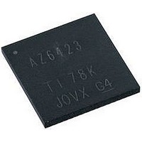
PIC24FJ128DA106-I/MR
Manufacturer Part Number
PIC24FJ128DA106-I/MR
Description
MCU PIC 16BIT FLASH 128K 64QFP
Manufacturer
Microchip Technology
Series
PIC® 24Fr
Specifications of PIC24FJ128DA106-I/MR
Core Size
16-Bit
Program Memory Size
128KB (43K x 24)
Core Processor
PIC
Speed
32MHz
Connectivity
I²C, IrDA, SPI, UART/USART, USB OTG
Peripherals
Brown-out Detect/Reset, GFX, LVD, POR, PWM, WDT
Number Of I /o
52
Program Memory Type
FLASH
Ram Size
24K x 8
Voltage - Supply (vcc/vdd)
2.2 V ~ 3.6 V
Data Converters
A/D 16x10b
Oscillator Type
Internal
Operating Temperature
-40°C ~ 85°C
Package / Case
64-VFQFN, Exposed Pad
Controller Family/series
PIC24
No. Of I/o's
52
Ram Memory Size
24KB
Cpu Speed
32MHz
No. Of Timers
5
No. Of Pwm Channels
9
Processor Series
PIC24FJ
Core
PIC
Data Bus Width
16 bit
Data Ram Size
24 KB
Interface Type
I2C, SPI, UART
Maximum Clock Frequency
32 MHz
Number Of Programmable I/os
29
Number Of Timers
5
Operating Supply Voltage
2.2 V to 3.6 V
Maximum Operating Temperature
+ 85 C
Mounting Style
SMD/SMT
3rd Party Development Tools
52713-733, 52714-737, 53276-922, EWDSPIC
Development Tools By Supplier
PG164130, DV164035, DV244005, DV164005, AC164127-4, AC164127-6, AC164139, DM240312, DV164039
Minimum Operating Temperature
- 40 C
On-chip Adc
10 bit, 16 Channel
Lead Free Status / RoHS Status
Lead free / RoHS Compliant
Eeprom Size
-
Lead Free Status / Rohs Status
Details


REGISTER 18-13: U1CNFG2: USB CONFIGURATION REGISTER 2
2010 Microchip Technology Inc.
bit 15
bit 7
Legend:
R = Readable bit
-n = Value at POR
bit 15-6
bit 5
bit 4
bit 3
bit 2
bit 1
bit 0
Note 1:
U-0
U-0
—
—
Never change these bits while the USBPWR bit is set (U1PWRC<0> = 1).
Unimplemented: Read as ‘0’
UVCMPSEL: V
1 = Use V
0 = Use V
PUVBUS: V
1 = Pull-up on V
0 = Pull-up on V
EXTI2CEN: I
1 = External module(s) is controlled via the I
0 = External module(s) controlled via the dedicated pins
UVBUSDIS: On-Chip 5V Boost Regulator Builder Disable bit
1 = On-chip boost regulator builder is disabled; digital output control interface is enabled
0 = On-chip boost regulator builder is active
UVCMPDIS: On-Chip V
1 = On-chip charge V
0 = On-chip charge V
UTRDIS: On-Chip Transceiver Disable bit
1 = On-chip transceiver is disabled; digital transceiver interface is enabled
0 = On-chip transceiver is active
U-0
U-0
—
—
BUSVLD
CMPST
BUS
2
C™ Interface For External Module Control Enable bit
W = Writable bit
‘1’ = Bit is set
UVCMPSEL
BUS
Pull-Up Enable bit
BUS
BUS
1 and V
, SESSVLD and SESSEND as comparator interface pins
R/W-0
U-0
Comparator External Interface Selection bit
—
pin is enabled
pin is disabled
BUS
BUS
BUS
CMPST
comparator is disabled; digital input status interface is enabled
comparator is active
Comparator Disable bit
2 as comparator interface pins
PUVBUS
PIC24FJ256DA210 FAMILY
R/W-0
U-0
—
(1)
U = Unimplemented bit, read as ‘0’
‘0’ = Bit is cleared
2
EXTI2CEN
C™ interface
R/W-0
U-0
—
(1)
UVBUSDIS
(1)
R/W-0
U-0
—
(1)
UVCMPDIS
x = Bit is unknown
R/W-0
U-0
—
DS39969B-page 263
(1)
UTRDIS
R/W-0
U-0
—
bit 8
bit 0
(1)
Related parts for PIC24FJ128DA106-I/MR
Image
Part Number
Description
Manufacturer
Datasheet
Request
R

Part Number:
Description:
Manufacturer:
Microchip Technology Inc.
Datasheet:
Part Number:
Description:
Manufacturer:
Microchip Technology Inc.
Datasheet:
Part Number:
Description:
Manufacturer:
Microchip Technology Inc.
Datasheet:
Part Number:
Description:
Manufacturer:
Microchip Technology Inc.
Datasheet:
Part Number:
Description:
Manufacturer:
Microchip Technology Inc.
Datasheet:
Part Number:
Description:
Manufacturer:
Microchip Technology Inc.
Datasheet:
Part Number:
Description:
Manufacturer:
Microchip Technology Inc.
Datasheet:
Part Number:
Description:
Manufacturer:
Microchip Technology Inc.
Datasheet: