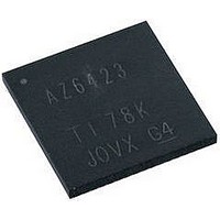
PIC24FJ128DA106-I/MR Microchip Technology, PIC24FJ128DA106-I/MR Datasheet - Page 288

PIC24FJ128DA106-I/MR
Manufacturer Part Number
PIC24FJ128DA106-I/MR
Description
MCU PIC 16BIT FLASH 128K 64QFP
Manufacturer
Microchip Technology
Series
PIC® 24Fr
Specifications of PIC24FJ128DA106-I/MR
Core Size
16-Bit
Program Memory Size
128KB (43K x 24)
Core Processor
PIC
Speed
32MHz
Connectivity
I²C, IrDA, SPI, UART/USART, USB OTG
Peripherals
Brown-out Detect/Reset, GFX, LVD, POR, PWM, WDT
Number Of I /o
52
Program Memory Type
FLASH
Ram Size
24K x 8
Voltage - Supply (vcc/vdd)
2.2 V ~ 3.6 V
Data Converters
A/D 16x10b
Oscillator Type
Internal
Operating Temperature
-40°C ~ 85°C
Package / Case
64-VFQFN, Exposed Pad
Controller Family/series
PIC24
No. Of I/o's
52
Ram Memory Size
24KB
Cpu Speed
32MHz
No. Of Timers
5
No. Of Pwm Channels
9
Processor Series
PIC24FJ
Core
PIC
Data Bus Width
16 bit
Data Ram Size
24 KB
Interface Type
I2C, SPI, UART
Maximum Clock Frequency
32 MHz
Number Of Programmable I/os
29
Number Of Timers
5
Operating Supply Voltage
2.2 V to 3.6 V
Maximum Operating Temperature
+ 85 C
Mounting Style
SMD/SMT
3rd Party Development Tools
52713-733, 52714-737, 53276-922, EWDSPIC
Development Tools By Supplier
PG164130, DV164035, DV244005, DV164005, AC164127-4, AC164127-6, AC164139, DM240312, DV164039
Minimum Operating Temperature
- 40 C
On-chip Adc
10 bit, 16 Channel
Lead Free Status / RoHS Status
Lead free / RoHS Compliant
Eeprom Size
-
Lead Free Status / Rohs Status
Details
- Current page: 288 of 408
- Download datasheet (4Mb)
PIC24FJ256DA210 FAMILY
REGISTER 20-1:
REGISTER 20-2:
DS39969B-page 288
bit 7-0
Note 1:
bit 15
bit 7
Legend:
R = Readable bit
-n = Value at POR
bit 15-2
bit 1
bit 0
Note 1:
U-0
U-0
—
—
2:
3:
The RCFGCAL register is only affected by a POR.
A write to the RTCEN bit is only allowed when RTCWREN = 1.
This bit is read-only. It is cleared to ‘0’ on a write to the lower half of the MINSEC register.
To enable the actual RTCC output, the RTCOE (RCFGCAL<10>) bit must also be set.
CAL<7:0>: RTC Drift Calibration bits
01111111 = Maximum positive adjustment; adds 508 RTC clock pulses every one minute
.
.
.
11111111 = Minimum negative adjustment; subtracts 4 RTC clock pulses every one minute
00000001 = Minimum positive adjustment; adds 4 RTC clock pulses every one minute
00000000 = No adjustment
.
.
.
10000000 = Maximum negative adjustment; subtracts 512 RTC clock pulses every one minute
Unimplemented: Read as ‘0’
RTSECSEL: RTCC Seconds Clock Output Select bit
1 = RTCC seconds clock is selected for the RTCC pin
0 = RTCC alarm pulse is selected for the RTCC pin
PMPTTL: EPMP Module TTL Input Buffer Select bit
1 = EPMP module inputs (PMDx, PMCS1) use TTL input buffers
0 = EPMP module inputs use Schmitt Trigger input buffers
U-0
U-0
—
—
RCFGCAL: RTCC CALIBRATION AND CONFIGURATION REGISTER
PADCFG1: PAD CONFIGURATION CONTROL REGISTER
W = Writable bit
‘1’ = Bit is set
U-0
U-0
—
—
U-0
U-0
—
—
U = Unimplemented bit, read as ‘0’
‘0’ = Bit is cleared
U-0
U-0
—
—
(1)
U-0
U-0
—
—
2010 Microchip Technology Inc.
x = Bit is unknown
RTSECSEL
R/W-0
U-0
—
(1)
(1)
PMPTTL
R/W-0
U-0
—
bit 8
bit 0
Related parts for PIC24FJ128DA106-I/MR
Image
Part Number
Description
Manufacturer
Datasheet
Request
R

Part Number:
Description:
Manufacturer:
Microchip Technology Inc.
Datasheet:

Part Number:
Description:
Manufacturer:
Microchip Technology Inc.
Datasheet:

Part Number:
Description:
Manufacturer:
Microchip Technology Inc.
Datasheet:

Part Number:
Description:
Manufacturer:
Microchip Technology Inc.
Datasheet:

Part Number:
Description:
Manufacturer:
Microchip Technology Inc.
Datasheet:

Part Number:
Description:
Manufacturer:
Microchip Technology Inc.
Datasheet:

Part Number:
Description:
Manufacturer:
Microchip Technology Inc.
Datasheet:

Part Number:
Description:
Manufacturer:
Microchip Technology Inc.
Datasheet:


