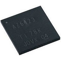
PIC24FJ128DA106-I/MR Microchip Technology, PIC24FJ128DA106-I/MR Datasheet - Page 297

PIC24FJ128DA106-I/MR
Manufacturer Part Number
PIC24FJ128DA106-I/MR
Description
MCU PIC 16BIT FLASH 128K 64QFP
Manufacturer
Microchip Technology
Series
PIC® 24Fr
Specifications of PIC24FJ128DA106-I/MR
Core Size
16-Bit
Program Memory Size
128KB (43K x 24)
Core Processor
PIC
Speed
32MHz
Connectivity
I²C, IrDA, SPI, UART/USART, USB OTG
Peripherals
Brown-out Detect/Reset, GFX, LVD, POR, PWM, WDT
Number Of I /o
52
Program Memory Type
FLASH
Ram Size
24K x 8
Voltage - Supply (vcc/vdd)
2.2 V ~ 3.6 V
Data Converters
A/D 16x10b
Oscillator Type
Internal
Operating Temperature
-40°C ~ 85°C
Package / Case
64-VFQFN, Exposed Pad
Controller Family/series
PIC24
No. Of I/o's
52
Ram Memory Size
24KB
Cpu Speed
32MHz
No. Of Timers
5
No. Of Pwm Channels
9
Processor Series
PIC24FJ
Core
PIC
Data Bus Width
16 bit
Data Ram Size
24 KB
Interface Type
I2C, SPI, UART
Maximum Clock Frequency
32 MHz
Number Of Programmable I/os
29
Number Of Timers
5
Operating Supply Voltage
2.2 V to 3.6 V
Maximum Operating Temperature
+ 85 C
Mounting Style
SMD/SMT
3rd Party Development Tools
52713-733, 52714-737, 53276-922, EWDSPIC
Development Tools By Supplier
PG164130, DV164035, DV244005, DV164005, AC164127-4, AC164127-6, AC164139, DM240312, DV164039
Minimum Operating Temperature
- 40 C
On-chip Adc
10 bit, 16 Channel
Lead Free Status / RoHS Status
Lead free / RoHS Compliant
Eeprom Size
-
Lead Free Status / Rohs Status
Details
- Current page: 297 of 408
- Download datasheet (4Mb)
21.0
FIGURE 21-1:
FIGURE 21-2:
2010 Microchip Technology Inc.
Note:
Note 1: n = PLEN<4:1> + 1.
Shift Buffer
32-BIT PROGRAMMABLE
CYCLIC REDUNDANCY CHECK
(CRC) GENERATOR
CRCDATH
Data
This data sheet summarizes the features
of this group of PIC24F devices. It is not
intended to be a comprehensive reference
source. For more information, refer to the
“PIC24F
Section
Cyclic
(DS39729). The information in this data
sheet supersedes the information in the
FRM.
(4x32, 8x16 or 16x8)
CRC Shift Engine
Variable FIFO
Shift Buffer
Redundancy
41.
Family
CRC BLOCK DIAGRAM
CRC SHIFT ENGINE DETAIL
X0
CRCDATL
“32-Bit
Reference
Bit 0
Check
Shifter Clock
Programmable
2 * F
LENDIAN
CY
1
0
Manual”,
CRCWDATH
(CRC)”
PIC24FJ256DA210 FAMILY
X1
Read/ W rite Bus
CRCWDATH
CRC Shift Engine
Bit 1
The 32-bit programmable CRC generator provides a
hardware implemented method of quickly generating
checksums for various networking and security
applications. It offers the following features:
• User-programmable CRC polynomial equation,
• Programmable shift direction (little or big-endian)
• Independent data and polynomial lengths
• Configurable interrupt output
• Data FIFO
Figure 21-1 displays a simplified block diagram of the
CRC generator. A simple version of the CRC shift
engine is displayed in Figure 21-2.
up to 32 bits
FIFO Empty
Event
CRCWDATL
CRCWDATL
Xn
(1)
Complete
Event
Shift
CRCISEL
DS39969B-page 297
Bit n
1
0
(1)
Interrupt
CRC
Related parts for PIC24FJ128DA106-I/MR
Image
Part Number
Description
Manufacturer
Datasheet
Request
R

Part Number:
Description:
Manufacturer:
Microchip Technology Inc.
Datasheet:

Part Number:
Description:
Manufacturer:
Microchip Technology Inc.
Datasheet:

Part Number:
Description:
Manufacturer:
Microchip Technology Inc.
Datasheet:

Part Number:
Description:
Manufacturer:
Microchip Technology Inc.
Datasheet:

Part Number:
Description:
Manufacturer:
Microchip Technology Inc.
Datasheet:

Part Number:
Description:
Manufacturer:
Microchip Technology Inc.
Datasheet:

Part Number:
Description:
Manufacturer:
Microchip Technology Inc.
Datasheet:

Part Number:
Description:
Manufacturer:
Microchip Technology Inc.
Datasheet:


