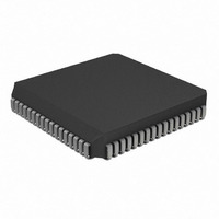
PIC17LC752-08I/L Microchip Technology, PIC17LC752-08I/L Datasheet - Page 117

PIC17LC752-08I/L
Manufacturer Part Number
PIC17LC752-08I/L
Description
IC MCU OTP 8KX16 A/D 68PLCC
Manufacturer
Microchip Technology
Series
PIC® 17Cr
Specifications of PIC17LC752-08I/L
Core Processor
PIC
Core Size
8-Bit
Speed
8MHz
Connectivity
I²C, SPI, UART/USART
Peripherals
Brown-out Detect/Reset, POR, PWM, WDT
Number Of I /o
50
Program Memory Size
16KB (8K x 16)
Program Memory Type
OTP
Ram Size
678 x 8
Voltage - Supply (vcc/vdd)
3 V ~ 5.5 V
Data Converters
A/D 12x10b
Oscillator Type
External
Operating Temperature
-40°C ~ 85°C
Package / Case
68-PLCC
Processor Series
PIC17LC
Core
PIC
Data Bus Width
8 bit
Data Ram Size
678 B
Interface Type
I2C, MSSP, RS- 232, SCI, SPI, USART
Maximum Clock Frequency
8 MHz
Number Of Programmable I/os
50
Number Of Timers
8
Operating Supply Voltage
3 V to 5.5 V
Maximum Operating Temperature
+ 85 C
Mounting Style
SMD/SMT
Development Tools By Supplier
ICE2000, DM173001
Minimum Operating Temperature
- 40 C
On-chip Adc
12 bit
Lead Free Status / RoHS Status
Lead free / RoHS Compliant
Eeprom Size
-
Lead Free Status / Rohs Status
Details
Available stocks
Company
Part Number
Manufacturer
Quantity
Price
Company:
Part Number:
PIC17LC752-08I/L
Manufacturer:
MICROCHIP
Quantity:
12 000
Company:
Part Number:
PIC17LC752-08I/L
Manufacturer:
Microchip Technology
Quantity:
10 000
- Current page: 117 of 304
- Download datasheet (6Mb)
14.0
Each USART module is a serial I/O module. There are
two USART modules that are available on the
PIC17C7XX. They are specified as USART1 and
USART2. The description of the operation of these mod-
ules is generic in regard to the register names and pin
names used. Table 14-1 shows the generic names that
are used in the description of operation and the actual
names for both USART1 and USART2. Since the control
bits in each register have the same function, their names
are the same (there is no need to differentiate).
The Transmit Status and Control Register (TXSTA) is
shown in Figure 14-1, while the Receive Status and
Control Register (RCSTA) is shown in Figure 14-2.
REGISTER 14-1:
2000 Microchip Technology Inc.
bit 7
bit 6
bit 5
bit 4
bit 3-2
bit 1
bit 0
UNIVERSAL SYNCHRONOUS
ASYNCHRONOUS RECEIVER
TRANSMITTER (USART)
MODULES
CSRC: Clock Source Select bit
Synchronous mode:
1 = Master mode (clock generated internally from BRG)
0 = Slave mode (clock from external source)
Asynchronous mode:
Don’t care
TX9: 9-bit Transmit Select bit
1 = Selects 9-bit transmission
0 = Selects 8-bit transmission
TXEN: Transmit Enable bit
1 = Transmit enabled
0 = Transmit disabled
SREN/CREN overrides TXEN in SYNC mode
SYNC: USART Mode Select bit
(Synchronous/Asynchronous)
1 = Synchronous mode
0 = Asynchronous mode
Unimplemented: Read as '0'
TRMT: Transmit Shift Register (TSR) Empty bit
1 = TSR empty
0 = TSR full
TX9D: 9th bit of Transmit Data (can be used to calculate the parity in software)
Legend:
R = Readable bit
- n = Value at POR Reset
bit 7
TXSTA1 REGISTER (ADDRESS: 15h, BANK 0)
TXSTA2 REGISTER (ADDRESS: 15h, BANK 4)
R/W-0
CSRC
R/W-0
TX9
R/W-0
TXEN
W = Writable bit
’1’ = Bit is set
R/W-0
SYNC
TABLE 14-1:
Generic Name
RCREG
SPBRG
TXREG
RCSTA
TXSTA
RX/DT
TX/CK
RCIE
RCIF
TXIE
TXIF
U = Unimplemented bit, read as ‘0’
’0’ = Bit is cleared
U-0
—
Interrupt Control Bits
USART MODULE GENERIC
NAMES
USART1 Name USART2 Name
RA4/RX1/DT1
RA5/TX1/CK1
Registers
U-0
RCREG1
SPBRG1
TXREG1
—
RCSTA1
TXSTA1
PIC17C7XX
RC1IE
RC1IF
TX1IE
TX1IF
Pins
x = Bit is unknown
TRMT
R-1
DS30289B-page 117
RG6/RX2/DT2
RG7/TX2/CK2
RCREG2
SPBRG2
TXREG2
RCSTA2
TXSTA2
RC2IE
RC2IF
TX2IE
TX2IF
R/W-x
TX9D
bit 0
Related parts for PIC17LC752-08I/L
Image
Part Number
Description
Manufacturer
Datasheet
Request
R

Part Number:
Description:
IC MCU OTP 8KX16 A/D 68PLCC
Manufacturer:
Microchip Technology
Datasheet:

Part Number:
Description:
IC MCU OTP 8KX16 A/D 64TQFP
Manufacturer:
Microchip Technology
Datasheet:

Part Number:
Description:
IC MCU OTP 8KX16 A/D 64TQFP
Manufacturer:
Microchip Technology
Datasheet:

Part Number:
Description:
Manufacturer:
Microchip Technology Inc.
Datasheet:

Part Number:
Description:
Manufacturer:
Microchip Technology Inc.
Datasheet:

Part Number:
Description:
Manufacturer:
Microchip Technology Inc.
Datasheet:

Part Number:
Description:
Manufacturer:
Microchip Technology Inc.
Datasheet:

Part Number:
Description:
Manufacturer:
Microchip Technology Inc.
Datasheet:

Part Number:
Description:
Manufacturer:
Microchip Technology Inc.
Datasheet:

Part Number:
Description:
Manufacturer:
Microchip Technology Inc.
Datasheet:


