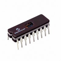
PIC16CE624/JW Microchip Technology, PIC16CE624/JW Datasheet - Page 47

PIC16CE624/JW
Manufacturer Part Number
PIC16CE624/JW
Description
IC MCU EPROM1KX14 EE COMP 18CDIP
Manufacturer
Microchip Technology
Series
PIC® 16Cr
Datasheet
1.PIC16CE623-04P.pdf
(113 pages)
Specifications of PIC16CE624/JW
Core Processor
PIC
Core Size
8-Bit
Speed
20MHz
Peripherals
Brown-out Detect/Reset, POR, WDT
Number Of I /o
13
Program Memory Size
1.75KB (1K x 14)
Program Memory Type
EPROM, UV
Eeprom Size
128 x 8
Ram Size
96 x 8
Voltage - Supply (vcc/vdd)
3 V ~ 5.5 V
Oscillator Type
External
Operating Temperature
0°C ~ 70°C
Package / Case
18-CDIP (0.300", 7.62mm) Window
For Use With
DVA16XP180 - ADAPTER DEVICE FOR MPLAB-ICEAC164010 - MODULE SKT PROMATEII DIP/SOIC
Lead Free Status / RoHS Status
Contains lead / RoHS non-compliant
Data Converters
-
Connectivity
-
- Current page: 47 of 113
- Download datasheet (2Mb)
9.0
The Voltage Reference is a 16-tap resistor ladder
network that provides a selectable voltage reference.
The resistor ladder is segmented to provide two ranges
of V
conserve power when the reference is not being used.
The VRCON register controls the operation of the
reference as shown in Register 9-1. The block diagram
is given in Figure 9-1.
REGISTER 9-1:
FIGURE 9-1:
1999 Microchip Technology Inc.
bit7
bit 7:
bit 6:
bit 5:
bit 4:
bit 3-0: V
V
R/W-0
REN
REF
V
Note:
REN
VOLTAGE REFERENCE
MODULE
values and has a power-down function to
V
V
V
Unimplemented: Read as ’0’
REN
ROE
RR
R
R is defined in Table 13-2.
R/W-0
<3:0>: V
V
: V
1 = V
0 = V
1 = V
0 = V
1 = Low Range
0 = High Range
when V
when V
ROE
: V
: V
V
VOLTAGE REFERENCE BLOCK DIAGRAM
REF
REF
REF
REF
VRCON REGISTER (ADDRESS 9Fh)
REF
REF
REF
REF
Range selection
REF
RR
RR
Enable
Output Enable
R/W-0
circuit powered on
circuit powered down, no I
is output on RA2 pin
is disconnected from RA2 pin
V
= 1: V
= 0: V
value selection 0
RR
8R
REF
REF
U-0
—
= (V
= 1/4 * V
R
R
<3:0>/ 24) * V
R/W-0
V
R3
DD
V
R
+ (V
R
[3:0]
DD
R
R/W-0
<3:0>/ 32) * V
V
16 Stages
drain
R2
DD
16-1 Analog Mux
15
9.1
The Voltage Reference can output 16 distinct voltage
levels for each range.
The equations used to calculate the output of the
Voltage Reference are as follows:
The setting time of the Voltage Reference must be
considered
(Table 13-1). Example 9-1 shows an example of how to
configure the Voltage Reference for an output voltage
of 1.25V with V
R/W-0
V
if V
if V
R1
R
RR
RR
DD
= 1: V
= 0: V
Configuring the Voltage Reference
R/W-0
V
R
when
R0
REF
REF
bit0
DD
= (V
= (V
= 5.0V.
PIC16CE62X
R = Readable bit
W = Writable bit
U = Unimplemented bit,
- n = Value at POR reset
changing
R
DD
<3:0>/24) x V
8R
x 1/4) + (V
read as ‘0’
V
V
R
R
3
0
(From VRCON<3:0>)
the
R
DS40182C-page 47
DD
<3:0>/32) x V
V
V
REF
RR
output
DD
Related parts for PIC16CE624/JW
Image
Part Number
Description
Manufacturer
Datasheet
Request
R

Part Number:
Description:
3.5KB Flash, 128B RAM, 18 I/O, CLC, CWG, DDS, 10-bit ADC 20 QFN 4x4mm TUBE
Manufacturer:
Microchip Technology
Datasheet:

Part Number:
Description:
3.5KB Flash, 128B RAM, 18 I/O, CLC, CWG, DDS, 10-bit ADC 20 PDIP .300in TUBE
Manufacturer:
Microchip Technology
Datasheet:

Part Number:
Description:
3.5KB Flash, 128B RAM, 18 I/O, CLC, CWG, DDS, 10-bit ADC 20 SOIC .300in TUBE
Manufacturer:
Microchip Technology
Datasheet:

Part Number:
Description:
3.5KB Flash, 128B RAM, 18 I/O, CLC, CWG, DDS, 10-bit ADC 20 SSOP .209in TUBE
Manufacturer:
Microchip Technology
Datasheet:

Part Number:
Description:
3.5KB Flash, 128B RAM, 18 I/O, CLC, CWG, DDS, 10-bit ADC 20 QFN 4x4mm TUBE
Manufacturer:
Microchip Technology
Datasheet:

Part Number:
Description:
3.5KB Flash, 128B RAM, 18 I/O, CLC, CWG, DDS, 10-bit ADC 20 PDIP .300in TUBE
Manufacturer:
Microchip Technology
Datasheet:

Part Number:
Description:
3.5KB Flash, 128B RAM, 18 I/O, CLC, CWG, DDS, 10-bit ADC 20 SOIC .300in TUBE
Manufacturer:
Microchip Technology
Datasheet:

Part Number:
Description:
3.5KB Flash, 128B RAM, 18 I/O, CLC, CWG, DDS, 10-bit ADC 20 SSOP .209in TUBE
Manufacturer:
Microchip Technology
Datasheet:

Part Number:
Description:
3.5KB Flash, 128B RAM, 18 I/O, CLC, CWG, DDS, 10-bit ADC 20 QFN 4x4mm T/R
Manufacturer:
Microchip Technology
Datasheet:

Part Number:
Description:
3.5KB Flash, 128B RAM, 18 I/O, CLC, CWG, DDS, 10-bit ADC 20 SOIC .300in T/R
Manufacturer:
Microchip Technology
Datasheet:

Part Number:
Description:
3.5KB Flash, 128B RAM, 18 I/O, CLC, CWG, DDS, 10-bit ADC 20 SSOP .209in T/R
Manufacturer:
Microchip Technology
Datasheet:

Part Number:
Description:
3.5KB Flash, 128B RAM, 18 I/O, CLC, CWG, DDS, 10-bit ADC 20 QFN 4x4mm TUBE
Manufacturer:
Microchip Technology
Datasheet:

Part Number:
Description:
3.5KB Flash, 128B RAM, 18 I/O, CLC, CWG, DDS, 10-bit ADC 20 PDIP .300in TUBE
Manufacturer:
Microchip Technology
Datasheet:

Part Number:
Description:
3.5KB Flash, 128B RAM, 18 I/O, CLC, CWG, DDS, 10-bit ADC 20 SOIC .300in TUBE
Manufacturer:
Microchip Technology
Datasheet:

Part Number:
Description:
3.5KB Flash, 128B RAM, 18 I/O, CLC, CWG, DDS, 10-bit ADC 20 SSOP .209in TUBE
Manufacturer:
Microchip Technology
Datasheet:


