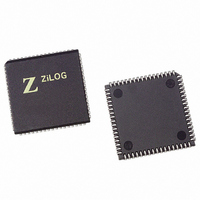
Z8F2422VS020SG Zilog, Z8F2422VS020SG Datasheet - Page 100

Z8F2422VS020SG
Manufacturer Part Number
Z8F2422VS020SG
Description
IC ENCORE MCU FLASH 24K 68PLCC
Manufacturer
Zilog
Series
Encore!® XP®r
Specifications of Z8F2422VS020SG
Core Processor
Z8
Core Size
8-Bit
Speed
20MHz
Connectivity
I²C, IrDA, SPI, UART/USART
Peripherals
Brown-out Detect/Reset, DMA, POR, PWM, WDT
Number Of I /o
46
Program Memory Size
24KB (24K x 8)
Program Memory Type
FLASH
Ram Size
2K x 8
Voltage - Supply (vcc/vdd)
3 V ~ 3.6 V
Data Converters
A/D 12x10b
Oscillator Type
Internal
Operating Temperature
0°C ~ 70°C
Package / Case
68-LCC (J-Lead)
Processor Series
Z8F242x
Core
eZ8
Data Bus Width
8 bit
Data Ram Size
2 KB
Interface Type
I2C, SPI, UART
Maximum Clock Frequency
20 MHz
Number Of Programmable I/os
46
Number Of Timers
4
Operating Supply Voltage
3 V to 3.6 V
Maximum Operating Temperature
+ 70 C
Mounting Style
SMD/SMT
Development Tools By Supplier
Z8F64200100KITG, ZENETSC0100ZACG, ZUSBSC00100ZACG, Z8F64210100ZDA, Z8F64210100ZDP, Z8F64210100ZDV, Z8F64220100ZDA, Z8F64220100ZDV, Z8F6422AR00ZEM, Z8F6422VS00ZEM, Z8F6421AN00ZEM
Minimum Operating Temperature
0 C
On-chip Adc
10 bit, 12 Channel
Lead Free Status / RoHS Status
Lead free / RoHS Compliant
Eeprom Size
-
Lead Free Status / Rohs Status
Details
Other names
269-4253
Z8F2422VS020SG
Z8F2422VS020SG
Available stocks
Company
Part Number
Manufacturer
Quantity
Price
- Current page: 100 of 297
- Download datasheet (9Mb)
Timer Control Register Definitions
PS019921-0308
Reading the Timer Count Values
Timer Output Signal Operation
Timer 0-3 High and Low Byte Registers
6. Write to the Timer Control 1 register to enable the timer.
7. Counting begins on the first appropriate transition of the Timer Input signal. No
In m/COMPARE mode, the elapsed time from timer start to Capture event can be calcu-
lated using the following equation:
The current count value in the timers can be read while counting (enabled). This capability
has no effect on timer operation. When the timer is enabled and the Timer High Byte
register is read, the contents of the Timer Low Byte register are placed in a holding
register. A subsequent read from the Timer Low Byte register returns the value in the
holding register. This operation allows accurate reads of the full 16-bit timer count value
while enabled. When the timers are not enabled, a read from the Timer Low Byte register
returns the actual value in the counter.
Timer Output is a GPIO Port pin alternate function. Generally, the Timer Output is toggled
every time the counter is reloaded.
Timers 0-2 are available in all packages. Timer 3 is only available in the 64-, 68-, and
80-pin packages.
The Timer 0-3 High and Low Byte (TxH and TxL) registers (see
page 87) contain the current 16-bit timer count value. When the timer is enabled, a read
from TxH causes the value in TxL to be stored in a temporary holding register. A read
from TMRL always returns this temporary register when the timers are enabled. When the
timer is disabled, reads from the TMRL reads the register directly.
Writing to the Timer High and Low Byte registers while the timer is enabled is not
recommended. There are no temporary holding registers available for write operations, so
simultaneous 16-bit writes are not possible. If either the Timer High or Low Byte registers
are written during counting, the 8-bit written value is placed in the counter (High or Low
Byte) at the next clock edge. The counter continues counting from the new value.
Timer 3 is unavailable in the 44-pin packages.
Capture Elapsed Time (s)
interrupt is generated by this first edge.
=
(
-------------------------------------------------------------------------------------------------- -
Capture Value Start Value
System Clock Frequency (Hz)
–
)
Z8 Encore! XP
×
Prescale
Product Specification
Table 39
®
and
F64XX Series
Table 40
Timers
on
86
Related parts for Z8F2422VS020SG
Image
Part Number
Description
Manufacturer
Datasheet
Request
R

Part Number:
Description:
Communication Controllers, ZILOG INTELLIGENT PERIPHERAL CONTROLLER (ZIP)
Manufacturer:
Zilog, Inc.
Datasheet:

Part Number:
Description:
KIT DEV FOR Z8 ENCORE 16K TO 64K
Manufacturer:
Zilog
Datasheet:

Part Number:
Description:
KIT DEV Z8 ENCORE XP 28-PIN
Manufacturer:
Zilog
Datasheet:

Part Number:
Description:
DEV KIT FOR Z8 ENCORE 8K/4K
Manufacturer:
Zilog
Datasheet:

Part Number:
Description:
KIT DEV Z8 ENCORE XP 28-PIN
Manufacturer:
Zilog
Datasheet:

Part Number:
Description:
DEV KIT FOR Z8 ENCORE 4K TO 8K
Manufacturer:
Zilog
Datasheet:

Part Number:
Description:
CMOS Z8 microcontroller. ROM 16 Kbytes, RAM 256 bytes, speed 16 MHz, 32 lines I/O, 3.0V to 5.5V
Manufacturer:
Zilog, Inc.
Datasheet:

Part Number:
Description:
Low-cost microcontroller. 512 bytes ROM, 61 bytes RAM, 8 MHz
Manufacturer:
Zilog, Inc.
Datasheet:

Part Number:
Description:
Z8 4K OTP Microcontroller
Manufacturer:
Zilog, Inc.
Datasheet:

Part Number:
Description:
CMOS SUPER8 ROMLESS MCU
Manufacturer:
Zilog, Inc.
Datasheet:

Part Number:
Description:
SL1866 CMOSZ8 OTP Microcontroller
Manufacturer:
Zilog, Inc.
Datasheet:

Part Number:
Description:
SL1866 CMOSZ8 OTP Microcontroller
Manufacturer:
Zilog, Inc.
Datasheet:

Part Number:
Description:
OTP (KB) = 1, RAM = 125, Speed = 12, I/O = 14, 8-bit Timers = 2, Comm Interfaces Other Features = Por, LV Protect, Voltage = 4.5-5.5V
Manufacturer:
Zilog, Inc.
Datasheet:

Part Number:
Description:
Manufacturer:
Zilog, Inc.
Datasheet:


