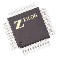
Z86E4312FSC Zilog, Z86E4312FSC Datasheet - Page 51

Z86E4312FSC
Manufacturer Part Number
Z86E4312FSC
Description
Z8 4K OTP 12 MHZ 44-PQFP
Manufacturer
Zilog
Series
Z8®r
Datasheet
1.Z86E3312SSC.pdf
(84 pages)
Specifications of Z86E4312FSC
Core Processor
Z8
Core Size
8-Bit
Speed
12MHz
Connectivity
EBI/EMI
Peripherals
POR, WDT
Number Of I /o
32
Program Memory Size
4KB (4K x 8)
Program Memory Type
OTP
Ram Size
236 x 8
Voltage - Supply (vcc/vdd)
3.5 V ~ 5.5 V
Oscillator Type
Internal
Operating Temperature
0°C ~ 70°C
Package / Case
44-LQFP
Data Bus Width
8 bit
Data Ram Size
236 B
Maximum Clock Frequency
12 MHz
Number Of Programmable I/os
32
Number Of Timers
2 bit
Operating Supply Voltage
3.5 V to 5.5 V
Maximum Operating Temperature
+ 70 C
Mounting Style
SMD/SMT
Minimum Operating Temperature
0 C
Lead Free Status / RoHS Status
Contains lead / RoHS non-compliant
Eeprom Size
-
Data Converters
-
Lead Free Status / Rohs Status
No
Other names
269-1108
Available stocks
Company
Part Number
Manufacturer
Quantity
Price
PS022901-0508
(Upper Byte)
After RESET
(Lower Byte)
4096/8192/16384
4095/8191/16383
First Byte of
Location of
Instruction
Executed
Interrupt
Interrupt
Vector
Vector
65535
12
11
10
9
8
7
6
5
4
3
2
1
0
EPROM Protect. When in ROM Protect Mode, and executing out of External Program
Memory, instructions LDC, LDCI, LDE, and LDEI cannot read Internal Program Mem-
ory.
When in EPROM Protect Mode and executing out of Internal Program Memory, instruc-
tions LDC, LDCI, LDE, and LDEI can read Internal Program Memory.
Data Memory (DM). In ROM Mode, the Z86E43/743/E44 can address up to 60156/48
KB of external data memory beginning at location 4096/8192/16384. In ROMless mode,
the Z86E43/743/E44 can address up to 64 KB of data memory. External data memory may
be included with, or separated from, the external program memory space. DM, an optional
I/0 function that can be programmed to appear on pin P34, is used to distinguish between
data and program memory space
the type of instruction being executed. An LDC opcode references PROGRAM (DM inac-
tive) memory, and an LDE instruction references data (DM active Low) memory.
ROM and RAM
ROM Module
On-Chip
EPROM
External
IRQ5
IRQ5
IRQ4
IRQ4
IRQ3
IRQ3
IRQ2
IRQ2
IRQ1
IRQ1
IRQ0
IRQ0
Figure 22. Program Memory Map
(Figure
23). The state of the DM signal is controlled by
(Z86E43/743/E44 Only)
ROMLess Module
ROM and RAM
CMOS Z8
External
IRQ5
IRQ5
IRQ4
IRQ4
IRQ3
IRQ3
IRQ2
IRQ2
IRQ1
IRQ1
IRQ0
IRQ0
®
Product Specification
OTP Microcontrollers
Electrical Characteristics
47


