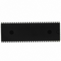
M38039G6HSP#U0 Renesas Electronics America, M38039G6HSP#U0 Datasheet - Page 64

M38039G6HSP#U0
Manufacturer Part Number
M38039G6HSP#U0
Description
IC 740/3803 MCU QZROM 64DIP
Manufacturer
Renesas Electronics America
Series
740/38000r
Datasheet
1.M38039G4HHPU0.pdf
(105 pages)
Specifications of M38039G6HSP#U0
Core Processor
740
Core Size
8-Bit
Speed
16.8MHz
Connectivity
SIO, UART/USART
Peripherals
LED, PWM, WDT
Number Of I /o
56
Program Memory Size
24KB (24K x 8)
Program Memory Type
QzROM
Ram Size
2K x 8
Voltage - Supply (vcc/vdd)
1.8 V ~ 5.5 V
Data Converters
A/D 16x10b; D/A 2x8b
Oscillator Type
Internal
Operating Temperature
-20°C ~ 85°C
Package / Case
64-SDIP (0.750", 19.05mm)
Lead Free Status / RoHS Status
Lead free / RoHS Compliant
Eeprom Size
-
3803 Group (Spec.H QzROM version)
REJ03B0166-0113 Rev.1.13
Page 62 of 100
A/D CONVERTER
[AD Conversion Register 1, 2] AD1, AD2
The AD conversion register is a read-only register that stores the
result of an A/D conversion. When reading this register during an
A/D conversion, the previous conversion result is read.
Bit 7 of the AD conversion register 2 is the conversion mode
selection bit. When this bit is set to “0”, the A/D converter
becomes the 10-bit A/D mode. When this bit is set to “1”, that
becomes the 8-bit A/D mode. The conversion result of the 8-bit
A/D mode is stored in the AD conversion register 1. As for 10-bit
A/D mode, not only 10-bit reading but also only high-order 8-bit
reading of conversion result can be performed by selecting the
reading procedure of the AD conversion registers 1, 2 after A/D
conversion is completed (in Figure 55).
As for 10-bit A/D mode, the 8-bit reading inclined to MSB is
performed when reading the AD converter register 1 after A/D
conversion is started; and when the AD converter register 1 is
read after reading the AD converter register 2, the 8-bit reading
inclined to LSB is performed.
[AD/DA Control Register] ADCON
The AD/DA control register controls the A/D conversion
process. Bits 0 to 2 and bit 4 select a specific analog input pin.
Bit 3 signals the completion of an A/D conversion. The value of
this bit remains at “0” during an A/D conversion, and changes to
“1” when an A/D conversion ends. Writing “0” to this bit starts
the A/D conversion.
[Comparison Voltage Generator]
The comparison voltage generator divides the voltage between
AV
voltage in the 10-bit A/D mode (256 division in 8-bit A/D mode).
The A/D converter successively compares the comparison
voltage Vref in each mode, dividing the V
below), with the input voltage.
• 10-bit A/D mode (10-bit reading)
• 10-bit A/D mode (8-bit reading)
• 8-bit A/D mode
[Channel Selector]
The channel selector selects one of ports P6
P0
[Comparator and Control Circuit]
The comparator and control circuit compares an analog input
voltage with the comparison voltage, and then stores the result in
the AD conversion registers 1, 2. When an A/D conversion is
completed, the control circuit sets the AD conversion completion
bit and the AD converter/Serial I/O3 transmit interrupt request
bit to “1”.
Note that because the comparator consists of a capacitor
coupling, set f(X
conversion.
Vref =
Vref =
Vref =
7
SS
/AN
and V
=0
15
V
-------------
V
-------------
V
-------------
1024
256
256
to P0
REF
REF
REF
REF
0
× n (n = 0 − 255)
/AN
× n (n = 0 − 1023)
× n (n − 0.5) (n = 1 − 255)
into 1024, and that outputs the comparison
IN )
8
, and inputs the voltage to the comparator.
to 500 kHz or more during an A/D
(n = 0)
Aug 21, 2009
7
/AN
REF
7
to P6
voltage (see
0
/AN
0
or
Fig 53. Structure of AD/DA control register
Fig 54. Structure of AD conversion register 2
Fig 55. Structure of 10-bit A/D mode reading
b7
b7
0
10-bit reading
(Read address 0038
AD conversion register 2
(AD2: address 0038
AD conversion register 1
(AD1: address 0035
8-bit reading
(Read only address 0035
AD conversion register 1
(AD1: address 0035
Note : Bits 2 to 6 of address 0038
b9
b0
16
16
16
16
)
)
)
b8
before 0035
b0
16
AD/DA control register
(ADCON : address 0034
Analog input pin selection bits 1
AD conversion completion bit
Analog input pin selection bit 2
Not used (returns “0” when read)
DA
DA
b2 b1 b0
16
0 0 0: P6
0 0 1: P6
0 1 0: P6
0 1 1: P6
1 0 0: P6
1 0 1: P6
1 1 0: P6
1 1 1: P6
0: Conversion in progress
1: Conversion completed
0: AN
1: AN
0: DA
1: DA
0: DA
1: DA
AD conversion register 2 (AD2)
(AD2: address 0038
)
become “0” at reading.
Not used (returns “0” when read)
Conversion mode selection bit
b7
b7
b9
b7
b7
1
2
0
output enable bit
output enable bit
0: 10-bit A/D conversion mode
1: 8-bit A/D conversion mode
b6 b5 b4 b3 b2 b1 b0
b8 b7 b6 b5 b4 b3 b2
0
8
1
1
2
2
to AN
to AN
output disabled
output enabled
output disabled
output enabled
16
0
1
2
3
4
5
6
7
)
/AN
/AN
/AN
/AN
/AN
/AN
/AN
/AN
7
15
side
0 or
1 or
2 or
3 or
4 or
5 or
6 or
7 or
side
16
b9 b8
)
P0
P0
P0
P0
P0
P0
P0
P0
b0
b0
b0
16
0
1
2
3
4
5
6
7
/AN
/AN
/AN
/AN
/AN
/AN
/AN
/AN
)
8
9
10
11
12
13
14
15


