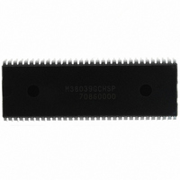
M38039GCHSP#U0 Renesas Electronics America, M38039GCHSP#U0 Datasheet - Page 74

M38039GCHSP#U0
Manufacturer Part Number
M38039GCHSP#U0
Description
IC 740/3803 MCU QZROM 64DIP
Manufacturer
Renesas Electronics America
Series
740/38000r
Datasheet
1.M38039G4HHPU0.pdf
(105 pages)
Specifications of M38039GCHSP#U0
Core Processor
740
Core Size
8-Bit
Speed
16.8MHz
Connectivity
SIO, UART/USART
Peripherals
LED, PWM, WDT
Number Of I /o
56
Program Memory Size
48KB (48K x 8)
Program Memory Type
QzROM
Ram Size
2K x 8
Voltage - Supply (vcc/vdd)
1.8 V ~ 5.5 V
Data Converters
A/D 16x10b; D/A 2x8b
Oscillator Type
Internal
Operating Temperature
-20°C ~ 85°C
Package / Case
64-SDIP (0.750", 19.05mm)
Lead Free Status / RoHS Status
Lead free / RoHS Compliant
Eeprom Size
-
- Current page: 74 of 105
- Download datasheet (2Mb)
3803 Group (Spec.H QzROM version)
REJ03B0166-0113 Rev.1.13
Page 72 of 100
QzROM Writing Mode
In the QzROM writing mode, the user ROM area can be
rewritten while the microcomputer is mounted on-board by using
a serial programmer which is applicable for this microcomputer.
Table 9 lists the pin description (QzROM writing mode) and
Figure 68 to Figure 70 show the pin connections.
Refer to Figure 71 and Figure 72 for examples of a connection
with a serial programmer.
Contact the manufacturer of your serial programmer for serial
programmer. Refer to the user ’s manual of your serial
programmer for details on how to use it.
Table 9
V
CNV
V
AV
RESET
X
X
P0
P1
P2
P3
P4
P5
P6
P4
P4
P4
CC
REF
IN
OUT
0
0
0
3
0
0
0
5
6
7
SS
− P0
− P1
− P2
− P3
, P4
− P5
− P6
, V
SS
Pin
SS
7
7
7
7
7
7
4
Pin description (QzROM writing mode)
Power source
V
Analog reference
voltage
Analog power source
Reset input
Clock input
Clock output
I/O port
ESDA input/output
ESCLK input
ESPGMB input
PP
input
Name
Aug 21, 2009
Output
Input
Input
Input
Input
Input
Input
Input
Input
I/O
I/O
I/O
Apply 2.7 to 5.5 V to V
QzROM programmable power source pin.
Input the reference voltage of A/D converter and D/A converter to
V
Connect AVss to Vss.
Reset input pin for active “L”. Reset occurs when RESET pin is
held at an “L” level for 16 cycles or more of X
Set the same termination as the single-chip mode.
Input “H” or “L” level signal or leave the pin open.
Serial data I/O pin.
Serial clock input pin.
Read/program pulse input pin.
REF
.
CC
, and 0 V to V
Function
SS
.
IN
.
Related parts for M38039GCHSP#U0
Image
Part Number
Description
Manufacturer
Datasheet
Request
R

Part Number:
Description:
KIT STARTER FOR M16C/29
Manufacturer:
Renesas Electronics America
Datasheet:

Part Number:
Description:
KIT STARTER FOR R8C/2D
Manufacturer:
Renesas Electronics America
Datasheet:

Part Number:
Description:
R0K33062P STARTER KIT
Manufacturer:
Renesas Electronics America
Datasheet:

Part Number:
Description:
KIT STARTER FOR R8C/23 E8A
Manufacturer:
Renesas Electronics America
Datasheet:

Part Number:
Description:
KIT STARTER FOR R8C/25
Manufacturer:
Renesas Electronics America
Datasheet:

Part Number:
Description:
KIT STARTER H8S2456 SHARPE DSPLY
Manufacturer:
Renesas Electronics America
Datasheet:

Part Number:
Description:
KIT STARTER FOR R8C38C
Manufacturer:
Renesas Electronics America
Datasheet:

Part Number:
Description:
KIT STARTER FOR R8C35C
Manufacturer:
Renesas Electronics America
Datasheet:

Part Number:
Description:
KIT STARTER FOR R8CL3AC+LCD APPS
Manufacturer:
Renesas Electronics America
Datasheet:

Part Number:
Description:
KIT STARTER FOR RX610
Manufacturer:
Renesas Electronics America
Datasheet:

Part Number:
Description:
KIT STARTER FOR R32C/118
Manufacturer:
Renesas Electronics America
Datasheet:

Part Number:
Description:
KIT DEV RSK-R8C/26-29
Manufacturer:
Renesas Electronics America
Datasheet:

Part Number:
Description:
KIT STARTER FOR SH7124
Manufacturer:
Renesas Electronics America
Datasheet:

Part Number:
Description:
KIT STARTER FOR H8SX/1622
Manufacturer:
Renesas Electronics America
Datasheet:

Part Number:
Description:
KIT DEV FOR SH7203
Manufacturer:
Renesas Electronics America
Datasheet:


