M30873FHGP#U5 Renesas Electronics America, M30873FHGP#U5 Datasheet - Page 280
M30873FHGP#U5
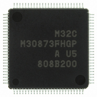
Manufacturer Part Number
M30873FHGP#U5
Description
IC M32C/87 MCU FLASH 100LQFP
Manufacturer
Renesas Electronics America
Series
M16C™ M32C/80r
Datasheet
1.M3087BFLGPU3.pdf
(629 pages)
Specifications of M30873FHGP#U5
Core Processor
M32C/80
Core Size
16/32-Bit
Speed
32MHz
Connectivity
CAN, EBI/EMI, I²C, IEBus, IrDA, SIO, UART/USART
Peripherals
DMA, POR, PWM, WDT
Number Of I /o
85
Program Memory Size
384KB (384K x 8)
Program Memory Type
FLASH
Ram Size
24K x 8
Voltage - Supply (vcc/vdd)
3 V ~ 5.5 V
Data Converters
A/D 26x10b; D/A 2x8b
Oscillator Type
Internal
Operating Temperature
-20°C ~ 85°C
Package / Case
100-LQFP
For Use With
R0K330879S001BE - KIT DEV RSK M32C/87R0K330879S000BE - KIT DEV RSK M32C/87
Lead Free Status / RoHS Status
Lead free / RoHS Compliant
Eeprom Size
-
Available stocks
Company
Part Number
Manufacturer
Quantity
Price

Part Number:
M30873FHGP#U5M30873FHGP#U3
Manufacturer:
Renesas Electronics America
Quantity:
10 000


M32C/87 Group (M32C/87, M32C/87A, M32C/87B)
REJ09B0180-0151 Rev.1.51 Jul 31, 2008
Page 256 of 587
Figure 17.27
Transmit/receive operation starts by writing data to UiTB register.
Read the UiRB register when the receive operation is completed.
i = 0 to 4
NOTES:
When an internal clock is used
1. Set to 0 in master mode, and set to 1 in slave mode.
2. The clock phase is determined by the combination of the CKPH and CKPOL bits in the UiSMR3 register.
3. Bits CNT3 to CNT0 select no division (n = 0) or divide-by-2n (n = 1 to 15).
I flag = 0
UiMR register: bits SMD2 to SMD0 = 001b
UiSMR register = 00h
UiSMR2 register = 00h
UiSMR3 register: SSE bit = 1
UiSMR4 register = 00h
UiC0 register: bits CLK1 to CLK0
UiBRG register = m
UiC1 register: TE bit = 0
SiTIC register: bits ILVL2 to ILVL0
SiRIC register: bits ILVL2 to ILVL0
I flag = 1
UiC1 register: TE bit = 1
Pin setting in the Function Select Registers
Register Settings in Special Mode 2
CRD bit = 1
NCH bit
CKPOL bit
UFORM bit
RE bit = 0
UiIRS bit
UiRRM bit = 0
UiLCH bit = 0
bit 7 = 0
RE bit = 1
CKDIR bit
IOPOL bit = 0
IR bit = 0
IR bit = 0
Start initial setting
End initial setting
CKPH bit
DINC bit
NODC bit = 0
bits DL2 to DL0 = 000b
Interrupt disabled
Clock synchronous mode
Clock select bit
SS function enabled
Clock phase set bit
Serial input pin set bit
UiBRG count source select bits
CTS function disabled
Data output select bit
CLK polarity select bit
Bit order select bit
m = 00h to FFh
Transmit operation disabled
Receive operation disabled
UARTi transmit interrupt souce select bit
Transmit interrupt priority level select bit
Interrupt not requested
Receive interrupt priority level select bit
Interrupt not requested
Interrupt enabled
Transmit operation enabled
Receive operation enabled
(1)
Baud rate =
(2)
(1)
(2)
17. Serial Interfaces (UART0 to UART4)
2(m + 1)
fj
fj: f1, f8, f2n
(3)
Related parts for M30873FHGP#U5
Image
Part Number
Description
Manufacturer
Datasheet
Request
R

Part Number:
Description:
KIT STARTER FOR M16C/29
Manufacturer:
Renesas Electronics America
Datasheet:

Part Number:
Description:
KIT STARTER FOR R8C/2D
Manufacturer:
Renesas Electronics America
Datasheet:

Part Number:
Description:
R0K33062P STARTER KIT
Manufacturer:
Renesas Electronics America
Datasheet:

Part Number:
Description:
KIT STARTER FOR R8C/23 E8A
Manufacturer:
Renesas Electronics America
Datasheet:

Part Number:
Description:
KIT STARTER FOR R8C/25
Manufacturer:
Renesas Electronics America
Datasheet:

Part Number:
Description:
KIT STARTER H8S2456 SHARPE DSPLY
Manufacturer:
Renesas Electronics America
Datasheet:

Part Number:
Description:
KIT STARTER FOR R8C38C
Manufacturer:
Renesas Electronics America
Datasheet:

Part Number:
Description:
KIT STARTER FOR R8C35C
Manufacturer:
Renesas Electronics America
Datasheet:

Part Number:
Description:
KIT STARTER FOR R8CL3AC+LCD APPS
Manufacturer:
Renesas Electronics America
Datasheet:
Part Number:
Description:
KIT STARTER FOR RX610
Manufacturer:
Renesas Electronics America
Datasheet:

Part Number:
Description:
KIT STARTER FOR R32C/118
Manufacturer:
Renesas Electronics America
Datasheet:

Part Number:
Description:
KIT DEV RSK-R8C/26-29
Manufacturer:
Renesas Electronics America
Datasheet:

Part Number:
Description:
KIT STARTER FOR SH7124
Manufacturer:
Renesas Electronics America
Datasheet:

Part Number:
Description:
KIT STARTER FOR H8SX/1622
Manufacturer:
Renesas Electronics America
Datasheet:

Part Number:
Description:
KIT DEV FOR SH7203
Manufacturer:
Renesas Electronics America
Datasheet: