M30873FHGP#U5 Renesas Electronics America, M30873FHGP#U5 Datasheet - Page 582
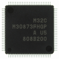
M30873FHGP#U5
Manufacturer Part Number
M30873FHGP#U5
Description
IC M32C/87 MCU FLASH 100LQFP
Manufacturer
Renesas Electronics America
Series
M16C™ M32C/80r
Datasheet
1.M3087BFLGPU3.pdf
(629 pages)
Specifications of M30873FHGP#U5
Core Processor
M32C/80
Core Size
16/32-Bit
Speed
32MHz
Connectivity
CAN, EBI/EMI, I²C, IEBus, IrDA, SIO, UART/USART
Peripherals
DMA, POR, PWM, WDT
Number Of I /o
85
Program Memory Size
384KB (384K x 8)
Program Memory Type
FLASH
Ram Size
24K x 8
Voltage - Supply (vcc/vdd)
3 V ~ 5.5 V
Data Converters
A/D 26x10b; D/A 2x8b
Oscillator Type
Internal
Operating Temperature
-20°C ~ 85°C
Package / Case
100-LQFP
For Use With
R0K330879S001BE - KIT DEV RSK M32C/87R0K330879S000BE - KIT DEV RSK M32C/87
Lead Free Status / RoHS Status
Lead free / RoHS Compliant
Eeprom Size
-
Available stocks
Company
Part Number
Manufacturer
Quantity
Price

Part Number:
M30873FHGP#U5M30873FHGP#U3
Manufacturer:
Renesas Electronics America
Quantity:
10 000


M32C/87 Group (M32C/87, M32C/87A, M32C/87B)
REJ09B0180-0151 Rev.1.51 Jul 31, 2008
Page 558 of 587
28.2
28.2.1
28.2.2
Table 28.3
NOTE:
Table 28.4
WDTS register
G0TB register
G0RI register
G1TB register
G1RI register
G2TB register
U5BRG register
U5TB register
U6BRG register
U6TB register
U1BRG register
U1TB register
U4BRG register
U4TB register
TA11 register
TA21 register
Transfer
Bit manipulation
Shift
Arithmetic
Logical
Jump
1. In one-shot timer mode and pulse width modulation mode only.
Set addresses 03CBh, 03CEh, 03CFh, 03D2h, and 03D3h to FFh after reset when using the 100-pin package.
Address 03DCh must be set to 00h after reset.
Table 28.3 lists registers containing write-only bits. Read-modify-write instructions cannot be used to set these
registers. If these registers are set using a read-modify-write instruction, undefined values are read from the
write-only bits in the register and written back to these bits. Table 28.4 lists read-modify-write instructions.
When establishing new values by modifying previous ones, write the previous values into RAM as well as to
the register. Change the contents of the RAM and then transfer the new values to the register.
Function
Special Function Registers (SFRs)
Register
100 Pin-Package
Register Settings
Registers with Write-Only Bits
Read-Modify-Write Instructions
MOVDir
BCLR, BMCnd, BNOT, BSET, BTSTC, BTSTS
ROLC, RORC, ROT, SHA, SHANC, SHL, SHLNC
ABS, ADC, ADCF, ADD, ADDX, DADC, DADD, DEC, DSBB, DSUB, EXTS, INC,
MUL, MULEX, MULU, NEG, SBB, SUB, SUBX
AND, NOT, OR, XOR
ADJNZ, SBJNZ
000Eh
00EAh
00ECh
012Ah
012Ch
016Dh to 016Ch
01C1h
01C3h to 01C2h
01C9h
01CBh to 01CAh
02E9h
02EBh to 02EAh
02F9h
02FBh to 02FAh
0303h to 0302h
0305h to 0304h
Address
TA41 register
DTT register
ICTB2 register
U3BRG register
U3TB register
U2BRG register
U2TB register
UDF register
TA0 register
TA1 register
TA2 register
TA3 register
TA4 register
U0BRG register
U0TB register
Mnemonic
Register
(1)
(1)
(1)
(1)
(1)
0329h
0307h to 0306h
030Ch
030Dh
032Bh to 032Ah
0339h
033Bh to 033Ah
0344h
0347h to 0346h
0349h to 0348h
034Bh to 034Ah
034Dh to 034Ch
034Fh to 034Eh
0369h
036Bh to 036Ah
Address
28. Usage Notes
Related parts for M30873FHGP#U5
Image
Part Number
Description
Manufacturer
Datasheet
Request
R

Part Number:
Description:
KIT STARTER FOR M16C/29
Manufacturer:
Renesas Electronics America
Datasheet:

Part Number:
Description:
KIT STARTER FOR R8C/2D
Manufacturer:
Renesas Electronics America
Datasheet:

Part Number:
Description:
R0K33062P STARTER KIT
Manufacturer:
Renesas Electronics America
Datasheet:

Part Number:
Description:
KIT STARTER FOR R8C/23 E8A
Manufacturer:
Renesas Electronics America
Datasheet:

Part Number:
Description:
KIT STARTER FOR R8C/25
Manufacturer:
Renesas Electronics America
Datasheet:

Part Number:
Description:
KIT STARTER H8S2456 SHARPE DSPLY
Manufacturer:
Renesas Electronics America
Datasheet:

Part Number:
Description:
KIT STARTER FOR R8C38C
Manufacturer:
Renesas Electronics America
Datasheet:

Part Number:
Description:
KIT STARTER FOR R8C35C
Manufacturer:
Renesas Electronics America
Datasheet:

Part Number:
Description:
KIT STARTER FOR R8CL3AC+LCD APPS
Manufacturer:
Renesas Electronics America
Datasheet:
Part Number:
Description:
KIT STARTER FOR RX610
Manufacturer:
Renesas Electronics America
Datasheet:

Part Number:
Description:
KIT STARTER FOR R32C/118
Manufacturer:
Renesas Electronics America
Datasheet:

Part Number:
Description:
KIT DEV RSK-R8C/26-29
Manufacturer:
Renesas Electronics America
Datasheet:

Part Number:
Description:
KIT STARTER FOR SH7124
Manufacturer:
Renesas Electronics America
Datasheet:

Part Number:
Description:
KIT STARTER FOR H8SX/1622
Manufacturer:
Renesas Electronics America
Datasheet:

Part Number:
Description:
KIT DEV FOR SH7203
Manufacturer:
Renesas Electronics America
Datasheet: