DS5003FPM-16+ Maxim Integrated Products, DS5003FPM-16+ Datasheet
DS5003FPM-16+
Specifications of DS5003FPM-16+


Related parts for DS5003FPM-16+

DS5003FPM-16+ Summary of contents
Page 1
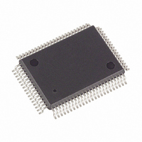
... Crash-Proof Operation Maintains All Nonvolatile Resources for Over 10 Years (at Room Temperature) in the Absence of Power Power-Fail Reset Early Warning Power-Fail Interrupt Watchdog Timer PART DS5003FPM-16+ + Denotes a lead(Pb)-free/RoHS-compliant package. Applications Pin Configuration appears at end of data sheet. Features Ordering Information INTERNAL TEMP ...
Page 2
Secure Microprocessor Chip ABSOLUTE MAXIMUM RATINGS Voltage Range on Any Pin Relative to Ground..................................-0. Voltage Range on V Relative CC to Ground ..........................................................-0.3V to +6.0V *Storage temperature is defined as the temperature of the device when V are ...
Page 3
DC CHARACTERISTICS (continued ±10 0°C to +70°C PARAMETER SYMBOL Output Low Voltage 3.2mA (P0.0–P0.7, ALE, OL BA0–BA14, BD0–BD7, R/W, CE1N, CE1–CE4, PE1–PE4, VRST) Output High Voltage -80μA ...
Page 4
Secure Microprocessor Chip AC CHARACTERISTICS—EXPANDED BUS-MODE TIMING SPECIFICATIONS ( ±10 0°C to +70°C.) (Figures PARAMETER SYMBOL Oscillator Frequency 1/t ALE Pulse Width Address Valid to ALE Low t Address Hold After ALE ...
Page 5
AC CHARACTERISTICS—POWER-CYCLE TIME ( ±10 0°C to +70°C.) (Figure PARAMETER Slew Rate from CCMIN LI Crystal Startup Time Power-On Reset Delay AC CHARACTERISTICS—SERIAL PORT TIMING (MODE ...
Page 6
Secure Microprocessor Chip AC CHARACTERISTICS—BYTE-WIDE ADDRESS/DATA BUS TIMING (continued ±10 0°C to +70°C.) (Figure PARAMETER Delay from R/W Low to Valid Data Out During MOVX (Write) Valid Data Out Hold Time from ...
Page 7
AC CHARACTERISTICS—PROG ( ±10 0°C to +70°C PARAMETER PROG Low to Active PROG High to Inactive Note 1: All voltages are referenced to ground. Note 2: Maximum operating I is measured with all output ...
Page 8
Secure Microprocessor Chip ALE WR t AVALL A7–A0 PORT 0 (Rn OR DPL) t AVRDL PORT 2 Figure 2. Expanded Data Memory Write Cycle t CLKHPW t CLKF Figure 3. External Clock Timing 8 _______________________________________________________________________________________ t t ALLRDL WRPW t ...
Page 9
PFW V CCMIN V LI INTERRUPT SERVICE ROUTINE CLOCK OSC INTERNAL RESET LITHIUM CURRENT Figure 4. Power-Cycle Timing _______________________________________________________________________________________ Secure Microprocessor Chip CSV t POR 9 ...
Page 10
Secure Microprocessor Chip 0 1 ALE CLOCK t DOCH DATA OUT 0 WRITE TO SBUF REGISTER INPUT DATA VALID CLEAR RI Figure 5. Serial Port Timing (Mode 0) MACHINE CYCLE XTAL2 ALE R/W BA0–BA14 PC OUT ...
Page 11
DATA DATA DACK RD t ACC WR DATA t ACD DRQ t CRQ Figure 7. RPC Timing Mode ______________________________________________________________________________________ Secure Microprocessor Chip READ OPERATION ...
Page 12
Secure Microprocessor Chip PIN NAME 13 V Power Supply, + Output. This is switched between V CC When power is above the lithium input, power is drawn from CCO isolated from a load. When V ...
Page 13
PIN NAME 37 BA0 35 BA1 33 BA2 30 BA3 28 BA4 26 BA5 Byte-Wide Address Bus Bits 14–0. This bus is combined with the nonmultiplexed data bus (BD7–BD0) to access external SRAM. Decoding is performed using CE1–CE4. Therefore, BA15 ...
Page 14
Secure Microprocessor Chip PIN NAME Active-Low Chip-Enable 4. This chip enable is provided to access a fourth 32kB block of CE4 62 memory. It connects to the chip-enable input of one SRAM. When MSEL = 0, this signal is unused. ...
Page 15
Detailed Description The DS5003 implements a security system that loads and executes application software in encrypted form 128kB of standard SRAM (64kB program + 64kB data) can be accessed by its byte-wide bus. This SRAM is converted by ...
Page 16
Secure Microprocessor Chip XTAL1 OSC XTAL2 TIMING RST AND ALE BUS PROG CONTROL P0.7 P0.6 P0.5 P0.4 PORT 0 P0.3 P0.2 P0.1 P0.0 P1.7 P1.6 P1.5 P1.4 PORT 1 P1.3 P1.2 P1.1 P1.0 P2.7 P2.6 P2.5 P2.4 PORT 2 P2.3 ...
Page 17
Security Circuitry Figure 9 shows the on-chip functions associated with the DS5003’s software security feature. Encryption logic consists of an address encryptor and a data encryptor. Although each encryptor uses its own algorithm for encrypting data, both depend on the ...
Page 18
Secure Microprocessor Chip When the application software is executed, the DS5003’s internal CPU operates as normal. Logical addresses are calculated for op code fetch cycles and also data read and write operations. The DS5003 can perform address encryption on logical ...
Page 19
This action triggers several events that defeat tampering. First, the encryption key is instantaneously erased. Without the encryption key, the DS5003 can no longer decrypt the contents of the SRAM. Therefore, the application software can no longer be correctly ...
Page 20
Secure Microprocessor Chip be read out and transmitted back to the host PC in decrypted form. Similarly, execution of the Verify com- mand within the same bootstrap session causes the incoming absolute hex data to be compared against the true ...
Page 21
An alternate configuration allows dynamic partitioning of a 64kB space as shown in Figure 11. Selecting PES = 1 provides another 64kB of potential data storage or memory-mapped peripheral space ...
Page 22
Secure Microprocessor Chip FFFFh PARTITION 4000h 0000h LEGEND: = BYTE-WIDE PROGRAM (ENCRYPTED) Figure 12. Memory Map with PES = +3V LITHIUM DS5003 PORT 0 PORT 1 PORT 2 PORT 3 14 MSEL ...
Page 23
+3V LITHIUM DS5003 PORT 0 PORT 1 PORT 2 PORT 3 14 +5V MSEL Figure 14. Connection to 64kB x 8 SRAM Power Management The DS5003 monitors V to provide power-fail reset, CC ...
Page 24
... Maxim cannot assume responsibility for use of any circuitry other than circuitry entirely embodied in a Maxim product. No circuit patent licenses are implied. Maxim reserves the right to change the circuitry and specifications without notice at any time. 24 ____________________Maxim Integrated Products, 120 San Gabriel Drive, Sunnyvale, CA 94086 408-737-7600 © 2008 Maxim Integrated Products ...