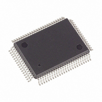
DS5003FPM-16+ Maxim Integrated Products, DS5003FPM-16+ Datasheet - Page 17

DS5003FPM-16+
Manufacturer Part Number
DS5003FPM-16+
Description
IC MICROPROCESSOR SECURE 80-MQFP
Manufacturer
Maxim Integrated Products
Series
DS500xr
Datasheet
1.DS5003-CS1.pdf
(24 pages)
Specifications of DS5003FPM-16+
Core Processor
8051
Core Size
8-Bit
Speed
16MHz
Connectivity
EBI/EMI, SIO, UART/USART
Peripherals
Power-Fail Reset, WDT
Number Of I /o
32
Program Memory Type
SRAM
Ram Size
256 x 8
Voltage - Supply (vcc/vdd)
4 V ~ 5.5 V
Oscillator Type
External
Operating Temperature
0°C ~ 70°C
Package / Case
80-MQFP, 80-PQFP
Processor Series
DS5003
Core
8051
Data Bus Width
8 bit
Program Memory Size
32 KB, 64 KB, 128 KB
Data Ram Size
32 KB, 64 KB, 128 KB
Interface Type
UART
Maximum Clock Frequency
16 MHz
Number Of Programmable I/os
32
Number Of Timers
2
Operating Supply Voltage
4.5 V to 5.5 V
Maximum Operating Temperature
+ 70 C
Mounting Style
SMD/SMT
3rd Party Development Tools
PK51, CA51, A51, ULINK2
Minimum Operating Temperature
0 C
Lead Free Status / RoHS Status
Lead free / RoHS Compliant
Eeprom Size
-
Program Memory Size
-
Data Converters
-
Lead Free Status / Rohs Status
Details
Figure 9 shows the on-chip functions associated with
the DS5003’s software security feature. Encryption logic
consists of an address encryptor and a data encryptor.
Although each encryptor uses its own algorithm for
encrypting data, both depend on the 64-bit key word
that is contained in the encryption key registers. Both
the encryptors operate during loading of the application
software and also during its execution.
The address encryptor translates each logical address,
i.e., the normal sequence of addresses that are gener-
ated in the logical flow of program execution, into an
encrypted address (or physical address) at which the
byte is actually stored. Each time a logical address is
generated, either during program loading or during
program execution, the address encryptor circuitry
uses the value of the 64-bit key word and of the
address itself to form the physical address, which are
presented on the address lines of the SRAM. The
encryption algorithm is such that there is one and only
one physical address for every possible logical
address. The address encryptor operates over the
Figure 9. Security Circuitry
BOOTSTRAP
PROGRAM
COUNTER
LOADER
______________________________________________________________________________________
SECURE INTERNAL ADDRESS BUS
SECURE INTERNAL DATA BUS
SECURITY
Security Circuitry
LOCK
GENERATOR
RANDOM-
NUMBER
POINTER
DATA
Secure Microprocessor Chip
64-BIT ENCRYPTION KEY
ENCRYPTOR
ENCRYPTOR
ADDRESS
entire memory range, which is configured during boot-
strap loading for access on the byte-wide bus.
As bootstrap loading of the application software is per-
formed, the data encryptor logic transforms the op
code, operand, or data byte at any given memory loca-
tion into an encrypted representation. As each byte is
read back to the CPU during program execution, the
internal data encryptor restores it to its original value.
When a byte is written to the external nonvolatile pro-
gram/data SRAM during program execution, that byte
is stored in encrypted form as well. The data encryption
logic uses the value of the 64-bit key, the logical
address to which the data is being written, and the
value of the data itself to form the encrypted data,
which is written to the nonvolatile program/data SRAM.
The encryption algorithm is repeatable, such that for a
given data value, encryption key value, and logical
address the encrypted byte is always the same.
However, there are many possible encrypted data val-
ues for each possible true-data value due to the algo-
rithm’s dependency on the values of the logical
address and encryption key.
DATA
ENCRYPTED BYTE-WIDE
ENCRYPTED BYTE-WIDE
ADDRESS BUS
DATA BUS
16
8
SDI
(SELF-DESTRUCT
INPUT)
BYTE-WIDE
EXTERNAL
RAM
17


