DS87C530-QNL Maxim Integrated Products, DS87C530-QNL Datasheet - Page 6
DS87C530-QNL
Manufacturer Part Number
DS87C530-QNL
Description
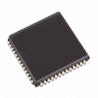
IC MCU EPR/ROM W/RTC 33MZ 52PLCC
Manufacturer
Maxim Integrated Products
Series
87Cr
Datasheet
1.DS87C530-QCL.pdf
(45 pages)
Specifications of DS87C530-QNL
Core Processor
8051
Core Size
8-Bit
Speed
33MHz
Connectivity
EBI/EMI, SIO, UART/USART
Peripherals
Power-Fail Reset, WDT
Number Of I /o
32
Program Memory Size
16KB (16K x 8)
Program Memory Type
OTP
Ram Size
1K x 8
Voltage - Supply (vcc/vdd)
4.5 V ~ 5.5 V
Oscillator Type
External
Operating Temperature
-40°C ~ 85°C
Package / Case
52-LCC, 52-PLCC
Processor Series
DS87C530
Core
8051
Data Bus Width
8 bit
Data Ram Size
1 KB
Interface Type
UART
Maximum Clock Frequency
33 MHz
Number Of Programmable I/os
32
Number Of Timers
3
Operating Supply Voltage
4.5 V to 5.5 V
Maximum Operating Temperature
+ 85 C
Mounting Style
SMD/SMT
3rd Party Development Tools
PK51, CA51, A51, ULINK2
Minimum Operating Temperature
- 40 C
Lead Free Status / RoHS Status
Contains lead / RoHS non-compliant
Eeprom Size
-
Data Converters
-
Other names
DS87C530QNL
Available stocks
Company
Part Number
Manufacturer
Quantity
Price
Company:

Part Number:
DS87C530-QNL
Manufacturer:
Maxim Integrated
Quantity:
10 000
Company:
Part Number:
DS87C530-QNL+
Manufacturer:
Maxim Integrated Products
Quantity:
135
Company:
Part Number:
DS87C530-QNL+
Manufacturer:
TI
Quantity:
111
Company:
Part Number:
DS87C530-QNL+
Manufacturer:
Maxim Integrated
Quantity:
10 000


PIN DESCRIPTION (continued)
2, 11, 13,
PLCC
14, 40,
30
31
32
33
34
35
36
37
15
16
17
18
19
20
21
22
42
51
27
28
41
PIN
4, 6, 7,
33, 34,
TQFP
23
24
25
26
27
28
29
30
10
11
12
13
14
15
35
44
20
21
47
8
9
P2.2 (AD10)
P2.3 (AD11)
P2.4 (AD12)
P2.5 (AD13)
P2.6 (AD14)
P2.7 (AD15)
P2.0 (AD8)
P2.1 (AD9)
RTCX2
RTCX1
NAME
V
N.C.
P3.0
P3.1
P3.2
P3.3
P3.4
P3.5
P3.6
P3.7
EA
BAT
Port 2 (A8–A15), I/O. Port 2 is a bidirectional I/O port. The reset condition of
Port 2 is logic high. In this state, a weak pullup holds the port high. This condition
also serves as an input mode, since any external circuit that writes to the port will
overcome the weak pullup. When software writes a 0 to any port pin, the device
will activate a strong pulldown that remains on until either a 1 is written or a reset
occurs. Writing a 1 after the port has been at 0 will cause a strong transition driver
to turn on, followed by a weaker sustaining pullup. Once the momentary strong
driver turns off, the port again becomes both the output high and input state. As an
alternate function Port 2 can function as MSB of the external address bus. This
bus can be used to read external ROM and read/write external RAM memory or
peripherals.
Port 3, I/O. Port 3 functions as both an 8-bit, bi-directional I/O port and an
alternate functional interface for external interrupts, Serial Port 0, Timer 0 and 1
Inputs, and RD and WR strobes. The reset condition of Port 3 is with all bits at a
logic 1. In this state, a weak pullup holds the port high. This condition also serves
as an input mode, since any external circuit that writes to the port will overcome
the weak pullup. When software writes a 0 to any port pin, the device will activate
a strong pulldown that remains on until either a 1 is written or a reset occurs.
Writing a 1 after the port has been at 0 will cause a strong transition driver to turn
on, followed by a weaker sustaining pullup. Once the momentary strong driver
turns off, the port again becomes both the output high and input state. The
alternate modes of Port 3 are outlined below.
Port
P3.0
P3.1
P3.2
P3.3
P3.4
P3.5
P3.6
P3.7
External Access Input, Active Low. Connect to ground to use an external ROM.
Internal RAM is still accessible as determined by register settings. Connect to V
to use internal ROM.
V
V
GND if battery will not be used with device.
Timekeeping Crystals. A 32.768kHz crystal between these pins supplies the time
base for the RTC. The devices support both 6pF and 12.5pF load capacitance
crystals as selected by an SFR bit (described later). To prevent noise from
affecting the RTC, the RTCX2 and RTCX1 pins should be guard-ringed with
GND2.
Not Connected. These pins should not be connected. They are reserved for use
with future devices in the family.
DS87C530/DS83C530 EPROM/ROM Microcontrollers with Real-Time Clock
BAT
CC
< V
Input. Connect to the power source that maintains SRAM and RTC when
BAT
Alternate
RXD0
TXD0
INT0
INT1
T0
T1
WR
RD
. Can be connected to a 3V lithium battery or a super cap. Connect to
6 of 45
Function
Serial Port 0 Input
Serial Port 0 Output
External Interrupt 0
External Interrupt 1
Timer 0 External Input
Timer 1 External Input
External Data Memory Write Strobe
External Data Memory Read Strobe
FUNCTION
CC
Related parts for DS87C530-QNL
Image
Part Number
Description
Manufacturer
Datasheet
Request
R

Part Number:
Description:
IC MCU EPR/ROM W/RTC 33MZ 52PLCC
Manufacturer:
Maxim Integrated Products
Datasheet:
Part Number:
Description:
IC MCU EPR/ROM W/RTC 33MZ 52PLCC
Manufacturer:
Maxim Integrated Products
Datasheet:
Part Number:
Description:
IC MCU EPR/ROM W/RTC 33MZ 52PLCC
Manufacturer:
Maxim Integrated Products
Datasheet:

Part Number:
Description:
IC MCU EPR/ROM W/RTC 33MZ 52TQFP
Manufacturer:
Maxim Integrated Products
Datasheet:
Part Number:
Description:
IC MCU EPR/ROM W/RTC 33MZ 52TQFP
Manufacturer:
Maxim Integrated Products
Datasheet:
Part Number:
Description:
IC MCU EPR/ROM W/RTC 33MZ 52TQFP
Manufacturer:
Maxim Integrated Products
Datasheet:
Part Number:
Description:
IC MCU EPR/ROM W/RTC 33MZ 52CLCC
Manufacturer:
Maxim Integrated Products
Datasheet:
Part Number:
Description:
MAX7528KCWPMaxim Integrated Products [CMOS Dual 8-Bit Buffered Multiplying DACs]
Manufacturer:
Maxim Integrated Products
Datasheet:
Part Number:
Description:
Single +5V, fully integrated, 1.25Gbps laser diode driver.
Manufacturer:
Maxim Integrated Products
Datasheet:
Part Number:
Description:
Single +5V, fully integrated, 155Mbps laser diode driver.
Manufacturer:
Maxim Integrated Products
Datasheet:
Part Number:
Description:
VRD11/VRD10, K8 Rev F 2/3/4-Phase PWM Controllers with Integrated Dual MOSFET Drivers
Manufacturer:
Maxim Integrated Products
Datasheet:
Part Number:
Description:
Highly Integrated Level 2 SMBus Battery Chargers
Manufacturer:
Maxim Integrated Products
Datasheet:
Part Number:
Description:
Current Monitor and Accumulator with Integrated Sense Resistor; ; Temperature Range: -40°C to +85°C
Manufacturer:
Maxim Integrated Products
Part Number:
Description:
TSSOP 14/A°/RS-485 Transceivers with Integrated 100O/120O Termination Resis
Manufacturer:
Maxim Integrated Products
Part Number:
Description:
TSSOP 14/A°/RS-485 Transceivers with Integrated 100O/120O Termination Resis
Manufacturer:
Maxim Integrated Products