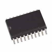
AT90S1200-12YC Atmel, AT90S1200-12YC Datasheet - Page 9

AT90S1200-12YC
Manufacturer Part Number
AT90S1200-12YC
Description
IC MCU 1K FLSH 12MHZ 20SSOP
Manufacturer
Atmel
Series
AVR® 90Sr
Datasheet
1.AT90S1200-12PC.pdf
(71 pages)
Specifications of AT90S1200-12YC
Core Processor
AVR
Core Size
8-Bit
Speed
12MHz
Connectivity
SPI
Peripherals
POR, WDT
Number Of I /o
15
Program Memory Size
1KB (512 x 16)
Program Memory Type
FLASH
Eeprom Size
64 x 8
Voltage - Supply (vcc/vdd)
4 V ~ 6 V
Oscillator Type
Internal
Operating Temperature
0°C ~ 70°C
Package / Case
20-SSOP
Lead Free Status / RoHS Status
Contains lead / RoHS non-compliant
Ram Size
-
Data Converters
-
Available stocks
Company
Part Number
Manufacturer
Quantity
Price
Part Number:
AT90S1200-12YC
Manufacturer:
AT
Quantity:
20 000
EEPROM Data Memory
Instruction Execution
Timing
0838H–AVR–03/02
The AT90S1200 contains 64 bytes of data EEPROM memory. It is organized as a sepa-
rate data space, in which single bytes can be read and written. The EEPROM has an
endurance of at least 100,000 write/erase cycles. The access between the EEPROM
and the CPU is described on page 25 specifying the EEPROM address register, the
EEPROM data register, and the EEPROM control register. For the SPI data download-
ing, see page 44 for a detailed description.
This section describes the general access timing concepts for instruction execution and
internal memory access.
The AVR CPU is driven by the System Clock Ø, directly generated from the external
clock crystal for the chip. No internal clock division is used.
Figure 11 shows the parallel instruction fetches and instruction executions enabled by
the Harvard architecture and the fast-access register file concept. This is the basic pipe-
lining concept to obtain up to 1 MIPS per MHz with the corresponding unique results for
functions per cost, functions per clocks, and functions per power-unit.
Figure 11. The Parallel Instruction Fetches and Instruction Executions
Figure 12 shows the internal timing concept for the register file. In a single clock cycle
an ALU operation using two register operands is executed, and the result is stored back
to the destination register.
Figure 12. Single-cycle ALU Operation
2nd Instruction Execute
Register Operands Fetch
3rd Instruction Execute
1st Instruction Execute
ALU Operation Execute
2nd Instruction Fetch
3rd Instruction Fetch
4th Instruction Fetch
1st Instruction Fetch
Total Execution Time
Result Write Back
System Clock Ø
System Clock Ø
T1
T1
T2
T2
T3
AT90S1200
T3
T4
T4
9


