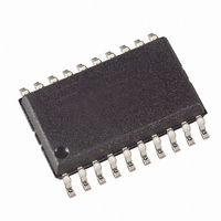
AT90S2313-10SI Atmel, AT90S2313-10SI Datasheet - Page 39

AT90S2313-10SI
Manufacturer Part Number
AT90S2313-10SI
Description
MCU 2K FLASH 10MHZ 20-SOIC
Manufacturer
Atmel
Series
AVR® 90Sr
Datasheet
1.AT90S2313-10PC.pdf
(92 pages)
Specifications of AT90S2313-10SI
Core Processor
AVR
Core Size
8-Bit
Speed
10MHz
Connectivity
SPI, UART/USART
Peripherals
Brown-out Detect/Reset, POR, PWM, WDT
Number Of I /o
15
Program Memory Size
2KB (1K x 16)
Program Memory Type
FLASH
Eeprom Size
128 x 8
Ram Size
128 x 8
Voltage - Supply (vcc/vdd)
4 V ~ 6 V
Oscillator Type
External
Operating Temperature
-40°C ~ 85°C
Package / Case
20-SOIC (7.5mm Width)
Lead Free Status / RoHS Status
Contains lead / RoHS non-compliant
Data Converters
-
Available stocks
Company
Part Number
Manufacturer
Quantity
Price
Company:
Part Number:
AT90S2313-10SI
Manufacturer:
ATMEL
Quantity:
5 510
Part Number:
AT90S2313-10SI
Manufacturer:
ATMEL/爱特梅尔
Quantity:
20 000
EEPROM Read/Write
Access
EEPROM Address Register –
EEAR
EEPROM Data Register –
EEDR
0839I–AVR–06/02
The EEPROM Access Registers are accessible in the I/O space.
The write access time is in the range of 2.5 - 4 ms, depending on the V
self-timing function, however, lets the user software detect when the next byte can be
written. If the user code contains code that writes the EEPROM, some precaution must
be taken. In heavily filtered power supplies, V
up/down. This causes the device for some period of time to run at a voltage lower than
specified as minimum for the clock frequency used. CPU operation under these condi-
tions may cause the Program Counter to perform unintentional jumps and eventually
execute the EEPROM write code. To secure EEPROM integrity, the user is advised to
use an external under-voltage reset circuit in this case.
In order to prevent unintentional EEPROM writes, a specific write procedure must be fol-
lowed. Refer to the description of the EEPROM Control Register for details on this.
When the EEPROM is written, the CPU is halted for two clock cycles before the next
instruction is executed. When the EEPROM is read, the CPU is halted for four clock
cycles before the next instruction is executed.
• Bit 7 – Res: Reserved Bit
This bit is a reserved bit in the AT90S2313 and will always read as zero.
• Bit 6..0 – EEAR6..0: EEPROM Address
The EEPROM Address Register (EEAR6..0) specifies the EEPROM address in the 128
bytes EEPROM space. The EEPROM data bytes are addressed linearly between 0 and
127.
• Bit 7..0 – EEDR7..0: EEPROM Data
For the EEPROM write operation, the EEDR Register contains the data to be written to
the EEPROM in the address given by the EEAR Register. For the EEPROM read oper-
ation, the EEDR contains the data read out from the EEPROM at the address given by
EEAR.
Bit
$1E ($3E)
Read/Write
Initial value
Bit
$1D ($3D)
Read/Write
Initial value
MSB
R/W
R
7
–
0
7
0
EEAR6
R/W
R/W
6
0
6
0
EEAR5
R/W
R/W
5
0
5
0
EEAR4
R/W
R/W
4
0
4
0
CC
EEAR3
R/W
R/W
3
0
3
0
is likely to rise or fall slowly on Power-
EEAR2
R/W
R/W
2
0
2
0
EEAR1
R/W
R/W
1
0
1
0
AT90S2313
EEAR0
R/W
LSB
R/W
CC
0
0
0
0
voltages. A
EEAR
EEDR
39


