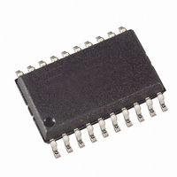
AT90S2313-10SI Atmel, AT90S2313-10SI Datasheet - Page 44

AT90S2313-10SI
Manufacturer Part Number
AT90S2313-10SI
Description
MCU 2K FLASH 10MHZ 20-SOIC
Manufacturer
Atmel
Series
AVR® 90Sr
Datasheet
1.AT90S2313-10PC.pdf
(92 pages)
Specifications of AT90S2313-10SI
Core Processor
AVR
Core Size
8-Bit
Speed
10MHz
Connectivity
SPI, UART/USART
Peripherals
Brown-out Detect/Reset, POR, PWM, WDT
Number Of I /o
15
Program Memory Size
2KB (1K x 16)
Program Memory Type
FLASH
Eeprom Size
128 x 8
Ram Size
128 x 8
Voltage - Supply (vcc/vdd)
4 V ~ 6 V
Oscillator Type
External
Operating Temperature
-40°C ~ 85°C
Package / Case
20-SOIC (7.5mm Width)
Lead Free Status / RoHS Status
Contains lead / RoHS non-compliant
Data Converters
-
Available stocks
Company
Part Number
Manufacturer
Quantity
Price
Company:
Part Number:
AT90S2313-10SI
Manufacturer:
ATMEL
Quantity:
5 510
Part Number:
AT90S2313-10SI
Manufacturer:
ATMEL/爱特梅尔
Quantity:
20 000
found to be logical “1”s, the start bit is rejected as a noise spike and the receiver starts
looking for the next 1-to-0 transition.
If, however, a valid start bit is detected, sampling of the data bits following the start bit is
performed. These bits are also sampled at samples 8, 9 and 10. The logical value found
in at least two of the three samples is taken as the bit value. All bits are shifted into the
Transmitter Shift Register as they are sampled. Sampling of an incoming character is
shown in Figure 36.
Figure 36. Sampling Received Data
When the stop bit enters the Receiver, the majority of the three samples must be “1” to
accept the stop bit. If two or more samples are logical “0”s, the Framing Error (FE) Flag
in the UART Status Register (USR) is set. Before reading the UDR Register, the user
should always check the FE bit to detect Framing Errors.
Whether or not a valid stop bit is detected at the end of a character-reception cycle, the
data is transferred to UDR and the RXC Flag in USR is set. UDR is in fact two physically
separate registers; one for transmitted data and one for received data. When UDR is
read, the Receive Data Register is accessed, and when UDR is written, the Transmit
Data Register is accessed. If 9-bit data word is selected (the CHR9 bit in the UART Con-
trol Register [UCR] is set), the RXB8 bit in UCR is loaded with bit 9 in the Transmit Shift
Register when data is transferred to UDR.
If, after having received a character, the UDR Register has not been read since the last
receive, the OverRun (OR) Flag in UCR is set. This means that the last data byte shifted
into the Shift Register could not be transferred to UDR and has been lost. The OR bit is
buffered and is updated when the valid data byte in UDR is read. Thus, the user should
always check the OR bit after reading the UDR Register in order to detect any overruns
if the baud rate is high or CPU load is high.
When the RXEN bit in the UCR Register is cleared (zero), the receiver is disabled. This
means that the PD0 pin can be used as a general I/O pin. When RXEN is set, the UART
Receiver will be connected to PD0, which is forced to be an input pin regardless of the
setting of the DDD0 bit in DDRD. When PD0 is forced to input by the UART, the
PORTD0 bit can still be used to control the pull-up resistor on the pin.
When the CHR9 bit in the UCR Register is set, transmitted and received characters are
nine bits long plus start and stop bits. The ninth data bit to be transmitted is the TXB8 bit
in UCR Register. This bit must be set to the wanted value before a transmission is initi-
ated by writing to the UDR Register. The ninth data bit received is the RXB8 bit in the
UCR Register.
AT90S2313
44
0839I–AVR–06/02


