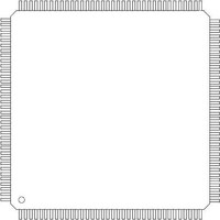
LH75411N0Q100C0 Sharp Microelectronics, LH75411N0Q100C0 Datasheet - Page 50

LH75411N0Q100C0
Manufacturer Part Number
LH75411N0Q100C0
Description
IC ARM7 BLUESTREAK MCU 144LQFP
Manufacturer
Sharp Microelectronics
Series
BlueStreak ; LH7r
Specifications of LH75411N0Q100C0
Core Processor
ARM7
Core Size
16/32-Bit
Speed
84MHz
Connectivity
EBI/EMI, SPI, SSI, SSP, UART/USART
Peripherals
Brown-out Detect/Reset, DMA, LCD, POR, PWM, WDT
Number Of I /o
76
Program Memory Type
ROMless
Ram Size
32K x 8
Voltage - Supply (vcc/vdd)
1.7 V ~ 3.6 V
Data Converters
A/D 8x10b
Oscillator Type
Internal
Operating Temperature
-40°C ~ 85°C
Package / Case
144-LQFP
Data Bus Width
32 bit
Data Ram Size
32 KB
Maximum Clock Frequency
84 MHz
Number Of Programmable I/os
8
Operating Supply Voltage
3 V to 3.6 V
Maximum Operating Temperature
+ 85 C
Mounting Style
SMD/SMT
Minimum Operating Temperature
- 40 C
Lead Free Status / RoHS Status
Lead free / RoHS Compliant
Eeprom Size
-
Program Memory Size
-
Lead Free Status / Rohs Status
Details
Available stocks
Company
Part Number
Manufacturer
Quantity
Price
Company:
Part Number:
LH75411N0Q100C0
Manufacturer:
Sharp Microelectronics
Quantity:
10 000
Company:
Part Number:
LH75411N0Q100C0,55
Manufacturer:
NXP Semiconductors
Quantity:
10 000
LH75400/01/10/11
UART 2 FEATURES
• Similar functionality to the industry-standard 82510
• Supported baud rates up to 3,225,600 baud (given a
• 5, 6, 7, 8, or 9 data bits per character
• Even, odd, HIGH, LOW, software, or no parity-bit
• 3/4, 1, 1-1/4, 1-1/2, 1-3/4, or 2 stop-bit generation
• μLAN address flag
• Full-duplex operation
• Separate transmit and receive FIFOs, with program-
• Two 16-bit baud-rate generators.
• One interrupt that can be triggered by transmit and
• Generation and detection of breaks during UART
• Support for local loopback, remote loopback, and
• μLAN Address Mode.
Timers
16-bit timers. The timers are clocked by the system
clock, but have an internal scaled-down system clock
that is used for the Pulse Width Modulator (PWM) and
compare functions.
scaled counter clock or external clock and can gener-
ate an overflow interrupt. All three timers have separate
internal prescaled counter clocks, with either a com-
mon external clock or a prescaled version of the sys-
tem clock.
• Timer 0 has five Capture Registers and two Com-
• Timer 1 and Timer 2 have two Capture and two Com-
and can generate an interrupt. The Compare Registers
can force the compare output pin either HIGH or LOW
upon a match.
50
system clock of 51.6096 MHz)
generation and detection
mable depth (1 or 4). Each FIFO has overrun protec-
tion and:
receive FIFO thresholds, receive errors, control
character or address marker reception, or timer
timeout
transactions
auto-echo modes
pare Registers.
pare Registers each.
– Programmable receive trigger levels: 1/4, 1/2,
– Programmable transmit trigger levels: empty, 1/4,
The LH75400/01/10/11 microcontrollers have three
All counters are incremented by an internal pre-
The Capture Registers have edge-selectable inputs
3/4, or full
1/2, 3/4.
Version 1.2
Controller Area Network (CAN)
Timer Compare Registers associated with a timer to
create a PWM. Each timer can generate a separate
interrupt. The interrupt becomes active if any enabled
compare, capture, or overflow interrupt condition
occurs. The interrupt remains active until all compare,
capture, and overflow interrupts are cleared.
Real Time Clock (RTC)
the APB. The RTC provides basic alarm functions or
acts as a long-time base counter by generating an inter-
rupt signal after counting for a programmed number of
cycles of an RTC input. Counting in 1-second intervals
is achieved using a 1 Hz clock input to the RTC.
RTC FEATURES
• 32-bit up-counter with programmable load
• Programmable 32-bit match Compare Register
• Software-maskable interrupt that is set when the
peripheral that connects as a slave to the APB. The
CAN Controller is located between the processor core
and a CAN Transceiver, and is accessed through the
AMBA port.
maximum frequency of 1MB/s, using the TX (transmit)
and RX (receive) lines. The TX and RX signals for data
transmission and reception provide the communications
interface between the CAN Controller and the CAN bus.
All peripherals share the TX and RX lines, and always
see the common incoming and outgoing data.
specifications. The bus is always controlled by the
node with the highest priority (lowest ID). Only after the
bus has been released can the next highest priority
node control it. Transmit and receive errors are han-
dled according to the CAN protocol.
the CAN Controller has two programmable Bus Timing
Registers that define timing parameters.
NOTE: The CAN Controller pertains to the LH75401 and LH75400
Counter and Compare Registers have identical values.
The timers support a PWM Mode that uses the two
The RTC is an AMBA slave module that connects to
The CAN 2.0B Controller is an AMBA-compliant
CAN communications are performed serially, at a
Bus arbitration follows the CAN 2.0A and CAN 2.0B
Bus timing is critical to the CAN protocol. Therefore,
microcontrollers.
System-on-Chip
Data Sheet


