DS87C550-QNL Maxim Integrated Products, DS87C550-QNL Datasheet - Page 12
DS87C550-QNL
Manufacturer Part Number
DS87C550-QNL
Description
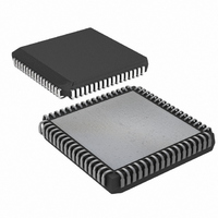
IC MCU EPROM ADC/PWM HS 68-PLCC
Manufacturer
Maxim Integrated Products
Series
87Cr
Datasheet
1.DS87C550-QNL.pdf
(49 pages)
Specifications of DS87C550-QNL
Core Processor
8051
Core Size
8-Bit
Speed
33MHz
Connectivity
EBI/EMI, SIO, UART/USART
Peripherals
Power-Fail Reset, PWM, WDT
Number Of I /o
55
Program Memory Size
8KB (8K x 8)
Program Memory Type
OTP
Ram Size
1K x 8
Voltage - Supply (vcc/vdd)
4.5 V ~ 5.5 V
Data Converters
A/D 6x10b
Oscillator Type
External
Operating Temperature
-40°C ~ 85°C
Package / Case
68-LCC, 68-PLCC
Lead Free Status / RoHS Status
Contains lead / RoHS non-compliant
Eeprom Size
-
Available stocks
Company
Part Number
Manufacturer
Quantity
Price
Company:

Part Number:
DS87C550-QNL
Manufacturer:
Maxim Integrated
Quantity:
10 000
Part Number:
DS87C550-QNL
Manufacturer:
DALLAS
Quantity:
20 000


DATA MEMORY ACCESS CONTROL Table 3
Notes on the status byte read at FFFCh with DME1, 0 = 1, 1: bits 2-0 reflect the programmed status of the
security lock bits LB2-LB0. They are individually set to a logic 1 to correspond to a security lock bit that
has been programmed. These status bits allow software to verify that the part has been locked before
running if desired. The bits are read only.
STRETCH MEMORY CYCLE
The DS87C550 allows software to adjust the speed of off-chip data memory and/or peripheral access by
adjusting the number of machine cycles it takes to execute a MOVX instruction. The micro is capable of
performing the MOVX in as little as two machine cycles. The on-chip SRAM uses this speed and any
MOVX instruction directed internally always uses two cycles. However, the time for the instruction
execution can be stretched for slower interface to external devices. This allows access to both fast
memory and slow memory or peripherals with no glue logic. Even in high-speed systems, it may not be
necessary or desirable to perform off-chip data memory access at full speed. In addition, there are a
variety of memory-mapped peripherals such as LCDs or UARTs that are slow and require more time to
access.
The Stretch MOVX function is controlled by the MD2-MD0 SFR bits in the Clock Control Register
(CKCON.2-0) as described below. They allow the user to select a Stretch value between 0 and 7. A
Stretch of 0 will result in a two-machine cycle MOVX instruction. A Stretch of 7 will result in a MOVX
of 12 machine cycles. Software can dynamically change the stretch value depending on the particular
memory or peripheral being accessed. The default stretch of one allows the use of commonly available
SRAMs without dramatically lengthening the memory access times.
Note that the STRETCH MOVX function is slightly different in the DS87C550 than in earlier members
of the high-speed microcontroller family. In all members of this family (including the DS87C550),
increasing the stretch value from 0 to 1 causes setup and hold times to be increased by 1 crystal clock
each. In older members of the family, there is no further change in setup and hold times regardless of the
number of stretch cycles selected. In the DS87C550 however, when a stretch value of 4 or above is
selected, the timing of the interface changes dramatically to allow for very slow peripherals. First, the
ALE signal is increased by 1 machine cycle. This increases the address setup time into the peripheral by
this amount. Next, the address is held on the bus for one additional machine cycle, increasing the address
hold time by this amount. The Read or Write signal is then increased by a machine cycle. Finally, the data
is held on the bus (for a write cycle) one additional machine cycle, thereby increasing the data hold time
by this amount. For every Stretch value greater than 4, the setup and hold times remain constant, and only
the width of the read or write signal is increased.
On reset, the Stretch value will default to a 1, resulting in a three-cycle MOVX for any external access.
Therefore, the default off-chip RAM access is not at full speed. This is a convenience to existing designs
DME1
0
0
1
1
DME0
0
1
0
1
DATA MEMORY ADDRESS
FFFDh - FFFFh
0400h – FFFBh
0000h - FFFFh
0400h - FFFFh
0000h - 03FFh
0000h - 03FFh
Reserved
FFFCh
12 of 49
External Data Memory *Default condition
Internal SRAM Data Memory
External Data Memory
Reserved
Internal SRAM Data Memory
Reserved - no external access
Read access to the status of lock bits
Reserved
MEMORY FUNCTION
Related parts for DS87C550-QNL
Image
Part Number
Description
Manufacturer
Datasheet
Request
R

Part Number:
Description:
IC MCU EPROM ADC/PWM HS 68-PLCC
Manufacturer:
Maxim Integrated Products
Datasheet:

Part Number:
Description:
Eprom High-speed Microcontroller With Adc And Pwm
Manufacturer:
Maxim Integrated Products, Inc.
Datasheet:

Part Number:
Description:
MAX7528KCWPMaxim Integrated Products [CMOS Dual 8-Bit Buffered Multiplying DACs]
Manufacturer:
Maxim Integrated Products
Datasheet:
Part Number:
Description:
Single +5V, fully integrated, 1.25Gbps laser diode driver.
Manufacturer:
Maxim Integrated Products
Datasheet:
Part Number:
Description:
Single +5V, fully integrated, 155Mbps laser diode driver.
Manufacturer:
Maxim Integrated Products
Datasheet:
Part Number:
Description:
VRD11/VRD10, K8 Rev F 2/3/4-Phase PWM Controllers with Integrated Dual MOSFET Drivers
Manufacturer:
Maxim Integrated Products
Datasheet:
Part Number:
Description:
Highly Integrated Level 2 SMBus Battery Chargers
Manufacturer:
Maxim Integrated Products
Datasheet:
Part Number:
Description:
Current Monitor and Accumulator with Integrated Sense Resistor; ; Temperature Range: -40°C to +85°C
Manufacturer:
Maxim Integrated Products
Part Number:
Description:
TSSOP 14/A°/RS-485 Transceivers with Integrated 100O/120O Termination Resis
Manufacturer:
Maxim Integrated Products
Part Number:
Description:
TSSOP 14/A°/RS-485 Transceivers with Integrated 100O/120O Termination Resis
Manufacturer:
Maxim Integrated Products
Part Number:
Description:
QFN 16/A°/AC-DC and DC-DC Peak-Current-Mode Converters with Integrated Step
Manufacturer:
Maxim Integrated Products
Part Number:
Description:
TDFN/A/65V, 1A, 600KHZ, SYNCHRONOUS STEP-DOWN REGULATOR WITH INTEGRATED SWI
Manufacturer:
Maxim Integrated Products
Part Number:
Description:
Integrated Temperature Controller f
Manufacturer:
Maxim Integrated Products
Part Number:
Description:
SOT23-6/I°/45MHz to 650MHz, Integrated IF VCOs with Differential Output
Manufacturer:
Maxim Integrated Products
Part Number:
Description:
SOT23-6/I°/45MHz to 650MHz, Integrated IF VCOs with Differential Output
Manufacturer:
Maxim Integrated Products