DS87C550-QNL Maxim Integrated Products, DS87C550-QNL Datasheet - Page 6
DS87C550-QNL
Manufacturer Part Number
DS87C550-QNL
Description
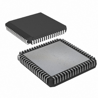
IC MCU EPROM ADC/PWM HS 68-PLCC
Manufacturer
Maxim Integrated Products
Series
87Cr
Datasheet
1.DS87C550-QNL.pdf
(49 pages)
Specifications of DS87C550-QNL
Core Processor
8051
Core Size
8-Bit
Speed
33MHz
Connectivity
EBI/EMI, SIO, UART/USART
Peripherals
Power-Fail Reset, PWM, WDT
Number Of I /o
55
Program Memory Size
8KB (8K x 8)
Program Memory Type
OTP
Ram Size
1K x 8
Voltage - Supply (vcc/vdd)
4.5 V ~ 5.5 V
Data Converters
A/D 6x10b
Oscillator Type
External
Operating Temperature
-40°C ~ 85°C
Package / Case
68-LCC, 68-PLCC
Lead Free Status / RoHS Status
Contains lead / RoHS non-compliant
Eeprom Size
-
Available stocks
Company
Part Number
Manufacturer
Quantity
Price
Company:

Part Number:
DS87C550-QNL
Manufacturer:
Maxim Integrated
Quantity:
10 000
Part Number:
DS87C550-QNL
Manufacturer:
DALLAS
Quantity:
20 000


PLCC/
CLCC
3-6, 32
33, 38
62-68
68
67
66
65
64
63
62
32
33
38
59
58
61
60
1,
1
4
5
6
3
28, 29
22, 30
33, 36
43, 44
62, 73
78, 79
64-71
74-77
3, 21
QFP
71
70
69
68
67
66
65
64
37
75
76
28
29
77
37
74
60
59
63
61
SIGNAL NAME
P5.0-P5.7
P6.0-P6.5
A
A
A
P6.7
A
NC
vref+
VCC
vref-
VSS
Port 5 - I/O. Port 5 functions as an open-drain 8-bit bi-directional I/O port or
alternately as an interface to the A/D converter. When used for general purpose
I/O, these pins operate in a quasi-bi-directional mode. Writing a logic 1 to these
pins (reset condition) will cause them to tri-state. This allows the pins to serve as
inputs since the tri-state condition can be overdriven by an external device. If a
logic 0 is written to a pin, it is pulled down internally and therefore serves as an
output pin containing a logic 0. Because these pins are open-drain, external pullup
resistors are required to create a logic 1 level when they are used as outputs. As
an alternate function Port 5 pins operate as the analog inputs for the A/D
converter as described below.
Port
P5.0
P5.1
P5.2
P5.3
P5.4
P5.5
P5.6
P5.7
Port 6 - I/O. Port 6 functions as a 7-bit bi-directional I/O port or alternately as an
interface to the PWM and A/D on-board peripherals. As an I/O port, these pins
operate as described in Port 1. Note that P6.6 is not implemented. The alternate
modes of Port 6 are detailed below.
Port
P6.0
P6.1
P6.2
P6.3
P6.4
P6.5
P6.7
A/D +Reference - Input. Supplies the positive reference voltage for the A/D
converter. This signal should be isolated from digital V
affecting A/D measurements.
A/D -Reference - Input. Supplies the negative reference voltage for the A/D
converter. This signal should be isolated from digital GND to prevent noise from
affecting A/D measurements.
Analog V
Analog Ground
NC-Reserved. These pins should not be connected. They are reserved for use
with future devices in this family.
Alternate Mode
ADC0
ADC1
ADC2
ADC3
ADC4
ADC5
ADC6
ADC7
Alternate Function
PWMO0
PWMO1
PWMO2
PWMO3
PWMC0
PWMC1
STADC
CC
6 of 49
Analog to Digital Converter input channel 1
Analog to Digital Converter input channel 2
Analog to Digital Converter input channel 3
Analog to Digital Converter input channel 4
Analog to Digital Converter input channel 5
Analog to Digital Converter input channel 6
Analog to Digital Converter input channel 7
PWM channel 0 output
PWM channel 1 output
PWM channel 2 output
PWM channel 3 output
PWM0 clock input
PWM1 clock input
External A/D conversion start signal (active low)
Analog to Digital Converter input channel 0
DESCRIPTION
CC
to prevent noise from
Related parts for DS87C550-QNL
Image
Part Number
Description
Manufacturer
Datasheet
Request
R

Part Number:
Description:
IC MCU EPROM ADC/PWM HS 68-PLCC
Manufacturer:
Maxim Integrated Products
Datasheet:

Part Number:
Description:
Eprom High-speed Microcontroller With Adc And Pwm
Manufacturer:
Maxim Integrated Products, Inc.
Datasheet:

Part Number:
Description:
MAX7528KCWPMaxim Integrated Products [CMOS Dual 8-Bit Buffered Multiplying DACs]
Manufacturer:
Maxim Integrated Products
Datasheet:
Part Number:
Description:
Single +5V, fully integrated, 1.25Gbps laser diode driver.
Manufacturer:
Maxim Integrated Products
Datasheet:
Part Number:
Description:
Single +5V, fully integrated, 155Mbps laser diode driver.
Manufacturer:
Maxim Integrated Products
Datasheet:
Part Number:
Description:
VRD11/VRD10, K8 Rev F 2/3/4-Phase PWM Controllers with Integrated Dual MOSFET Drivers
Manufacturer:
Maxim Integrated Products
Datasheet:
Part Number:
Description:
Highly Integrated Level 2 SMBus Battery Chargers
Manufacturer:
Maxim Integrated Products
Datasheet:
Part Number:
Description:
Current Monitor and Accumulator with Integrated Sense Resistor; ; Temperature Range: -40°C to +85°C
Manufacturer:
Maxim Integrated Products
Part Number:
Description:
TSSOP 14/A°/RS-485 Transceivers with Integrated 100O/120O Termination Resis
Manufacturer:
Maxim Integrated Products
Part Number:
Description:
TSSOP 14/A°/RS-485 Transceivers with Integrated 100O/120O Termination Resis
Manufacturer:
Maxim Integrated Products
Part Number:
Description:
QFN 16/A°/AC-DC and DC-DC Peak-Current-Mode Converters with Integrated Step
Manufacturer:
Maxim Integrated Products
Part Number:
Description:
TDFN/A/65V, 1A, 600KHZ, SYNCHRONOUS STEP-DOWN REGULATOR WITH INTEGRATED SWI
Manufacturer:
Maxim Integrated Products
Part Number:
Description:
Integrated Temperature Controller f
Manufacturer:
Maxim Integrated Products
Part Number:
Description:
SOT23-6/I°/45MHz to 650MHz, Integrated IF VCOs with Differential Output
Manufacturer:
Maxim Integrated Products
Part Number:
Description:
SOT23-6/I°/45MHz to 650MHz, Integrated IF VCOs with Differential Output
Manufacturer:
Maxim Integrated Products