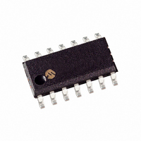
MCP6024-E/SL Microchip Technology, MCP6024-E/SL Datasheet - Page 20

MCP6024-E/SL
Manufacturer Part Number
MCP6024-E/SL
Description
IC OPAMP QUAD 2.5V 10MHZ 14SOIC
Manufacturer
Microchip Technology
Specifications of MCP6024-E/SL
Slew Rate
7 V/µs
Package / Case
14-SOIC (3.9mm Width), 14-SOL
Amplifier Type
General Purpose
Number Of Circuits
4
Output Type
Rail-to-Rail
Gain Bandwidth Product
10MHz
Current - Input Bias
1pA
Voltage - Input Offset
500µV
Current - Supply
1mA
Current - Output / Channel
30mA
Voltage - Supply, Single/dual (±)
2.5 V ~ 5.5 V
Operating Temperature
-40°C ~ 125°C
Mounting Type
Surface Mount
Number Of Channels
4
Common Mode Rejection Ratio (min)
70 dB
Input Offset Voltage
0.25 mV
Input Bias Current (max)
5000 pA
Operating Supply Voltage
3 V, 5 V
Supply Current
5.4 mA
Maximum Operating Temperature
+ 125 C
Minimum Operating Temperature
- 40 C
Mounting Style
SMD/SMT
Shutdown
No
Supply Voltage (max)
5.5 V
Supply Voltage (min)
2.5 V
Technology
CMOS
Voltage Gain Db
110 dB
Lead Free Status / RoHS Status
Lead free / RoHS Compliant
-3db Bandwidth
-
Lead Free Status / Rohs Status
Lead free / RoHS Compliant
Available stocks
Company
Part Number
Manufacturer
Quantity
Price
Company:
Part Number:
MCP6024-E/SL
Manufacturer:
INTERSIL
Quantity:
11 981
Part Number:
MCP6024-E/SL
Manufacturer:
MCIROCHIP
Quantity:
20 000
MCP6021/1R/2/3/4
4.9
In applications where low input bias current is critical,
PCB (printed circuit board) surface-leakage effects
need to be considered. Surface leakage is caused by
humidity, dust or other contamination on the board.
Under low humidity conditions, a typical resistance
between nearby traces is 10
cause 5 pA of current to flow, which is greater than the
MCP6021/1R/2/3/4 family’s bias current at +25°C
(1 pA, typical).
The easiest way to reduce surface leakage is to use a
guard ring around sensitive pins (or traces). The guard
ring is biased at the same voltage as the sensitive pin.
Figure 4-11
FIGURE 4-11:
Layout.
1.
2.
4.10
Due to their speed capabilities, a little extra care in the
PCB (Printed Circuit Board) layout can make a
significant difference in the performance of these op
amps. Good PC board layout techniques will help you
achieve the performance shown in Section 1.0 “Elec-
trical Characteristics” and Section 2.0 “Typical Per-
formance Curves”, while also helping you minimize
EMC (Electro-Magnetic Compatibility) issues.
Use a solid ground plane and connect the bypass local
capacitor(s) to this plane with minimal length traces.
This cuts down inductive and capacitive crosstalk.
DS21685D-page 20
Non-inverting Gain and Unity-Gain Buffer.
a)
b)
Inverting
Gain Amplifiers (convert current to voltage, such
as photo detectors).
a)
b)
Guard Ring
PCB Surface Leakage
Connect the guard ring to the inverting input
pin (V
common mode input voltage.
Connect the non-inverting pin (V
input with a wire that does not touch the
PCB surface.
Connect the guard ring to the non-inverting
input pin (V
to the same reference voltage as the op
amp’s input (e.g., V
Connect the inverting pin (V
with a wire that does not touch the PCB
surface.
High Speed PCB Layout
shows an example of this type of layout.
IN
(Figure
–); this biases the guard ring to the
IN
+). This biases the guard ring
Example Guard Ring
4-11) and Transimpedance
V
IN
– V
12
DD
Ω. A 5V difference would
IN
/2 or ground).
+
IN
–) to the input
IN
+) to the
Separate digital from analog, low speed from high
speed and low power from high power. This will reduce
interference.
Keep sensitive traces short and straight. Separating
them from interfering components and traces. This is
especially important for high-frequency (low rise-time)
signals.
Sometimes it helps to place guard traces next to victim
traces. They should be on both sides of the victim
trace, and as close as possible. Connect the guard
trace to ground plane at both ends, and in the middle
for long traces.
Use coax cables (or low inductance wiring) to route
signal and power to and from the PCB.
4.11
4.11.1
Figure 4-12
can be used as an A/D converter driver. It has a band-
width of 20 kHz and a reasonable step response. It will
work well for conversion rates of 80 ksps and greater (it
has 29 dB attenuation at 60 kHz).
FIGURE 4-12:
Anti-aliasing Filter with a 20 kHz Cutoff
Frequency.
This filter can easily be adjusted to another bandwidth
by multiplying all capacitors by the same factor.
Alternatively, the resistors can all be scaled by another
common factor to adjust the bandwidth.
8.45 kΩ
1.2 nF
Typical Applications
A/D CONVERTER DRIVER AND
ANTI-ALIASING FILTER
shows a third-order Butterworth filter that
14.7 kΩ
A/D Converter Driver and
© 2009 Microchip Technology Inc.
33.2 kΩ
100 pF
1.0 nF
MCP602X


