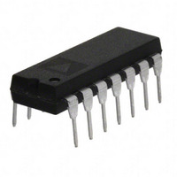
OP482GPZ Analog Devices Inc, OP482GPZ Datasheet - Page 3

OP482GPZ
Manufacturer Part Number
OP482GPZ
Description
IC OPAMP JFET 4MHZ QUAD LP 14DIP
Manufacturer
Analog Devices Inc
Specifications of OP482GPZ
Slew Rate
9 V/µs
Amplifier Type
General Purpose
Number Of Circuits
4
Gain Bandwidth Product
4MHz
Current - Input Bias
3pA
Voltage - Input Offset
200µV
Current - Supply
210µA
Current - Output / Channel
12mA
Voltage - Supply, Single/dual (±)
9 V ~ 36 V, ±4.5 V ~ 18 V
Operating Temperature
-40°C ~ 85°C
Mounting Type
Through Hole
Package / Case
14-DIP (0.300", 7.62mm)
Op Amp Type
Low Power
No. Of Amplifiers
4
Bandwidth
4MHz
Supply Voltage Range
± 4.5V To ± 18V
Amplifier Case Style
DIP
No. Of Pins
14
Operating Temperature Range
-40°C To +85°C
Common Mode Rejection Ratio
90
Current, Input Bias
3 pA
Current, Input Offset
1 pA
Current, Output
10 mA
Current, Supply
210 μA
Impedance, Thermal
39 °C/W
Number Of Amplifiers
Quad
Package Type
PDIP-14
Temperature, Operating, Range
-40 to +85 °C
Voltage, Gain
20 V/mV
Voltage, Input
-11 to +15 V
Voltage, Noise
36 nV/sqrt Hz
Voltage, Offset
0.2 mV
Voltage, Output, High
13.9 V
Voltage, Output, Low
-13.9 V
Voltage, Supply
±15 V
Lead Free Status / RoHS Status
Lead free / RoHS Compliant
Output Type
-
-3db Bandwidth
-
Lead Free Status / Rohs Status
RoHS Compliant part
Electrostatic Device
SPECIFICATIONS
ELECTRICAL CHARACTERISTICS
At V
Table 1.
Parameter
INPUT CHARACTERISTICS
OUTPUT CHARACTERISTICS
POWER SUPPLY
DYNAMIC PERFORMANCE
NOISE PERFORMANCE
1
The input bias and offset currents are characterized at T
Offset Voltage
Input Bias Current
Input Offset Current
Input Voltage Range
Common-Mode Rejection Ratio
Large Signal Voltage Gain
Offset Voltage Drift
Bias Current Drift
Output Voltage High
Output Voltage Low
Short-Circuit Limit
Open-Loop Output Impedance
Power Supply Rejection Ratio
Supply Current/Amplifier
Supply Voltage Range
Slew Rate
Full-Power Bandwidth
Settling Time
Gain Bandwidth Product
Phase Margin
Voltage Noise
Voltage Noise Density
Current Noise Density
S
= ±15.0 V, T
A
= 25°C, unless otherwise noted; applies to both A and G grade.
Symbol
V
V
I
I
CMRR
A
∆V
∆I
V
V
I
Z
PSRR
I
V
SR
BW
t
GBP
Ø
e
e
i
n
B
OS
SC
SY
S
OS
OS
OH
OL
OUT
S
n
n
VO
O
B
p-p
OS
/∆T
P
/∆T
A
= T
J
= 85°C. Bias and offset currents are guaranteed but not tested at −40°C.
Conditions
OP282
OP282, −40°C ≤ T
OP482
OP482, −40°C ≤ T
V
V
V
V
−11 V ≤ V
R
R
R
R
Source
Sink
f = 1 MHz
V
V
R
1% distortion
To 0.01%
0.1 Hz to 10 Hz
f = 1 kHz
L
L
L
L
L
CM
CM
CM
CM
S
O
= 10 kΩ
= 10 kΩ, −40°C ≤ T
= 10 kΩ
= 10 kΩ
= ±4.5 V to ±18 V, −40°C ≤ T
= 10 kΩ
= 0 V, −40°C ≤ T
= 0 V
= 0 V
= 0 V
= 0 V
Rev. F | Page 3 of 16
1
1
CM
≤ +15 V, −40°C ≤ T
A
A
A
≤ +85°C
≤ +85°C
≤ 85°C
A
≤ +85°C
A
A
≤ +85°C
≤ +85°C
Min
−11
70
20
15
+13.5
3
±4.5
7
Typ
0.2
0.2
3
1
90
10
8
+13.9
−13.9
10
−12
200
25
210
9
125
1.6
4
55
1.3
36
0.01
OP282/OP482
Max
3
4.5
4
6
100
500
50
250
+15
−13.5
−8
316
250
±18
Unit
mV
mV
mV
mV
pA
pA
pA
pA
dB
V/mV
V/mV
µV/°C
pA/°C
V
V
mA
mA
Ω
µV/V
µA
V
V/µs
kHz
µs
MHz
Degrees
µV p-p
nV/√Hz
pA/√Hz
V


