OP482GPZ Analog Devices Inc, OP482GPZ Datasheet - Page 4
OP482GPZ
Manufacturer Part Number
OP482GPZ
Description
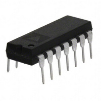
IC OPAMP JFET 4MHZ QUAD LP 14DIP
Manufacturer
Analog Devices Inc
Specifications of OP482GPZ
Slew Rate
9 V/µs
Amplifier Type
General Purpose
Number Of Circuits
4
Gain Bandwidth Product
4MHz
Current - Input Bias
3pA
Voltage - Input Offset
200µV
Current - Supply
210µA
Current - Output / Channel
12mA
Voltage - Supply, Single/dual (±)
9 V ~ 36 V, ±4.5 V ~ 18 V
Operating Temperature
-40°C ~ 85°C
Mounting Type
Through Hole
Package / Case
14-DIP (0.300", 7.62mm)
Op Amp Type
Low Power
No. Of Amplifiers
4
Bandwidth
4MHz
Supply Voltage Range
± 4.5V To ± 18V
Amplifier Case Style
DIP
No. Of Pins
14
Operating Temperature Range
-40°C To +85°C
Common Mode Rejection Ratio
90
Current, Input Bias
3 pA
Current, Input Offset
1 pA
Current, Output
10 mA
Current, Supply
210 μA
Impedance, Thermal
39 °C/W
Number Of Amplifiers
Quad
Package Type
PDIP-14
Temperature, Operating, Range
-40 to +85 °C
Voltage, Gain
20 V/mV
Voltage, Input
-11 to +15 V
Voltage, Noise
36 nV/sqrt Hz
Voltage, Offset
0.2 mV
Voltage, Output, High
13.9 V
Voltage, Output, Low
-13.9 V
Voltage, Supply
±15 V
Lead Free Status / RoHS Status
Lead free / RoHS Compliant
Output Type
-
-3db Bandwidth
-
Lead Free Status / Rohs Status
RoHS Compliant part
Electrostatic Device


OP282/OP482
ABSOLUTE MAXIMUM RATINGS
Table 2.
Parameters
Supply Voltage
Input Voltage
Differential Input Voltage
Output Short-Circuit Duration
Storage Temperature Range
Operating Temperature Range
Junction Temperature Range
Lead Temperature Range (Soldering 60 sec)
1
ESD CAUTION
ESD (electrostatic discharge) sensitive device. Electrostatic charges as high as 4000 V readily accumulate
on the human body and test equipment and can discharge without detection. Although this product features
proprietary ESD protection circuitry, permanent damage may occur on devices subjected to high energy
electrostatic discharges. Therefore, proper ESD precautions are recommended to avoid performance
degradation or loss of functionality.
For supply voltages less than ±18 V, the absolute maximum input voltage is
equal to the supply voltage.
P-Suffix (N), S-Suffix (R), RM Packages
OP282G, OP282A, OP482G
P-Suffix (N), S-Suffix (R), RM Packages
1
Ratings
±18 V
±18 V
36 V
Indefinite
−65°C to +150°C
−40°C to +85°C
−65°C to +150°C
300°C
Rev. F | Page 4 of 16
Stresses above those listed under Absolute Maximum Ratings
may cause permanent damage to the device. This is a stress
rating only; functional operation of the device at these or any
other conditions above those indicated in the operational
section of this specification is not implied. Exposure to absolute
maximum rating conditions for extended periods may affect
device reliability.
Table 3.
Package Type
8-Lead MSOP [RM]
8-Lead SOIC (S-Suffix) [R]
14-Lead PDIP (P-Suffix) [N]
14-Lead SOIC (S-Suffix) [R]
1
θ
socket for CERDIP, PDIP; θ
for SOIC or MSOP package.
JA
is specified for the worst-case conditions; i.e., θ
JA
is specified for device soldered in circuit board
θ
206
157
83
104
JA
1
JA
is specified for device in
θ
44
56
39
36
JC
Unit
°C/W
°C/W
°C/W
°C/W
Related parts for OP482GPZ
Image
Part Number
Description
Manufacturer
Datasheet
Request
R

Part Number:
Description:
±1.7g Dual-Axis IMEMS Accelerometer Evaluation Board
Manufacturer:
Analog Devices Inc
Datasheet:

Part Number:
Description:
Inertial Sensor Evaluation System
Manufacturer:
Analog Devices Inc
Datasheet:
Part Number:
Description:
Manufacturer:
Analog Devices Inc
Datasheet:
Part Number:
Description:
Manufacturer:
Analog Devices Inc
Datasheet:
Part Number:
Description:
Manufacturer:
Analog Devices Inc
Datasheet:
Part Number:
Description:
Manufacturer:
Analog Devices Inc
Datasheet:
Part Number:
Description:
Manufacturer:
Analog Devices Inc
Datasheet:
Part Number:
Description:
Manufacturer:
Analog Devices Inc
Datasheet:
Part Number:
Description:
Manufacturer:
Analog Devices Inc
Datasheet:
Part Number:
Description:
Manufacturer:
Analog Devices Inc
Datasheet:
Part Number:
Description:
Manufacturer:
Analog Devices Inc
Datasheet:
Part Number:
Description:
Manufacturer:
Analog Devices Inc
Datasheet:
Part Number:
Description:
Manufacturer:
Analog Devices Inc
Datasheet: